PIC12F510/16F506
5.4
I/O Interfacing
5.0
I/O PORT
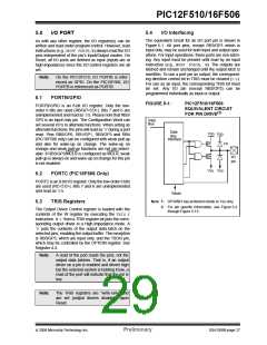
The equivalent circuit for an I/O port pin is shown in
Figure 5-1. All port pins, except RB3/GP3 which is
input only, may be used for both input and output oper-
ations. For input operations, these ports are non-latch-
ing. Any input must be present until read by an input
instruction (e.g., MOVF PORTB, W). The outputs are
latched and remain unchanged until the output latch is
rewritten. To use a port pin as output, the correspond-
ing direction control bit in TRIS must be cleared (= 0).
For use as an input, the corresponding TRIS bit must
be set. Any I/O pin (except RB3/GP3) can be
programmed individually as input or output.
As with any other register, the I/O register(s) can be
written and read under program control. However, read
instructions (e.g., MOVF PORTB, W) always read the I/O
pins independent of the pin’s Input/Output modes. On
Reset, all I/O ports are defined as input (inputs are at
high-impedance) since the I/O control registers are all
set.
Note:
On the PIC12F510, I/O PORTB is refer-
enced as GPIO. On the PIC16F506, I/O
PORTB is referenced as PORTB.
5.1
PORTB/GPIO
FIGURE 5-1:
PIC12F510/16F506
EQUIVALENT CIRCUIT
FOR PIN DRIVE(2)
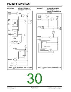
PORTB/GPIO is an 8-bit I/O register. Only the low-
order 6 bits are used (RB/GP<5:0>). Bits 7 and 6 are
unimplemented and read as ‘0’s. Please note that RB3/
GP3 is an input only pin. The Configuration Word can
set several I/O’s to alternate functions. When acting as
alternate functions, the pins will read as ‘0’ during a port
read. Pins RB0/GP0, RB1/GP1, RB3/GP3 and RB4
(PIC16F506 only) can be configured with weak pull-up
and also for wake-up on change. The wake-up on
change and weak pull-up functions are not pin select-
able. If RB3/GP3/MCLR is configured as MCLR, weak
pull-up is always on and wake-up on change for this pin
is not enabled.
Data
Bus
Data
Bus
Interface
VDD
P
VDD
(1)
N
I/O
pin
D
Q
VSS VSS
5.2
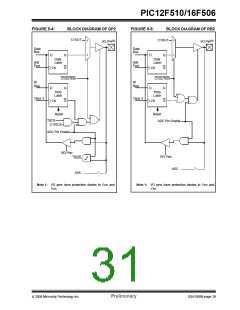
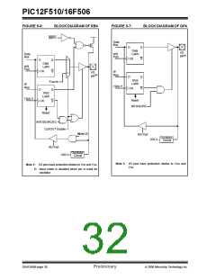
PORTC (PIC16F506 Only)
CK
Q
PORTC is an 8-bit I/O register. Only the low-order 6 bits
are used (RC<5:0>). Bits 7 and 6 are unimplemented
and read as ‘0’s.
Reset
Note 1: GP3/RB3 has protection diode to VSS only.
5.3
TRIS Registers
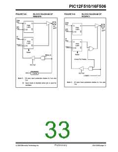
2: For pin specific information, see Figure 5-2
The Output Driver Control register is loaded with the
contents of the W register by executing the TRIS f
instruction. A ‘1’ from a TRIS register bit puts the corre-
sponding output driver in a High-Impedance mode. A
‘0’ puts the contents of the output data latch on the
selected pins, enabling the output buffer. The exception
is RB3/GP3, which are input only, and the T0CKI pin,
which may be controlled by the OPTION register. See
Register 4-3.
through Figure 5-13.
Note:
A read of the port reads the pins, not the
output data latches. That is, if an output
driver on a pin is enabled and driven high
but the external system is holding it low, a
read of the port will indicate that the pin is
low.
Note:
The TRIS registers are “write-only” and
are set (output drivers disabled) upon
Reset.
© 2006 Microchip Technology Inc.
Preliminary
DS41268B-page 27

 ETC [ ETC ]