PIC12F510/16F506
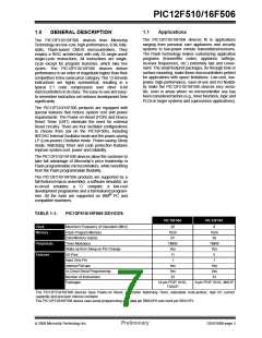
The ALU is 8 bits wide and capable of addition, subtrac-
tion, shift and logical operations. Unless otherwise
mentioned, arithmetic operations are two’s comple-
ment in nature. In two-operand instructions, one
operand is typically the W (working) register. The other
operand is either a file register or an immediate
constant. In single-operand instructions, the operand is
either the W register or a file register.
3.0
ARCHITECTURAL OVERVIEW
The high performance of the PIC12F510/16F506
devices can be attributed to a number of architectural
features commonly found in RISC microprocessors.
The PIC12F510/16F506 devices use a Harvard archi-
tecture in which program and data are accessed on
separate buses. This improves bandwidth over tradi-
tional von Neumann architectures where program and
data are fetched on the same bus. Separating program
and data memory further allows instructions to be sized
differently than the 8-bit wide data word. Instruction
opcodes are 12 bits wide, making it possible to have all
single-word instructions. A 12-bit wide program mem-
ory access bus fetches a 12-bit instruction in a single
cycle. A two-stage pipeline overlaps fetch and execu-
tion of instructions. Consequently, all instructions (33)
execute in a single cycle (200 ns @ 20 MHz, 1 μs @
4 MHz) except for program branches.
The W register is an 8-bit working register used for ALU
operations. It is not an addressable register.
Depending on the instruction executed, the ALU may
affect the values of the Carry (C), Digit Carry (DC) and
Zero (Z) bits in the STATUS register. The C and DC bits
operate as a borrow and digit borrow out bit, respec-
tively, in subtraction. See the SUBWF and ADDWF
instructions for examples.
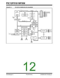
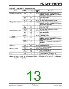
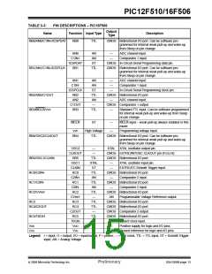
A simplified block diagram is shown in Figure 3-1 for
PIC12F510 with the corresponding device pins
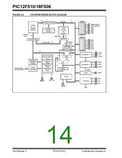
described in Table 3-2. A simplified block diagram for
PIC16F506 is shown in Figure 3-2 with the
corresponding device pins described in Table 3-3.
Table 3-1 lists program memory (Flash) and data
memory (RAM) for the PIC12F510/16F506 devices.
TABLE 3-1:
Device
PIC12F510/16F506 MEMORY
Memory
Program
Data
PIC12F510
PIC16F506
1024 x 12
1024 x 12
38 x 8
67 x 8
The PIC12F510/16F506 devices can directly or indi-
rectly address its register files and data memory. All
Special Function Registers (SFR), including the PC,
are mapped in the data memory. The PIC12F510/
16F506 devices have a highly orthogonal (symmetri-
cal) instruction set that makes it possible to carry out
any operation, on any register, using any addressing
mode. This symmetrical nature and lack of “special
optimal situations” make programming with the
PIC12F510/16F506 devices simple, yet efficient. In
addition, the learning curve is reduced significantly.
The PIC12F510/16F506 devices contain an 8-bit ALU
and working register. The ALU is a general purpose
arithmetic unit. It performs arithmetic and Boolean
functions between data in the working register and any
register file.
© 2006 Microchip Technology Inc.
Preliminary
DS41268B-page 9

 ETC [ ETC ]