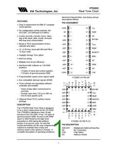
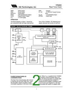
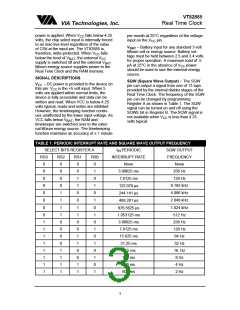
VT82885
Real Time Clock
VIA Technologies, Inc.
E. Periodic Interrupt Flag (PF) bit is cleared
to zero.
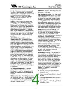
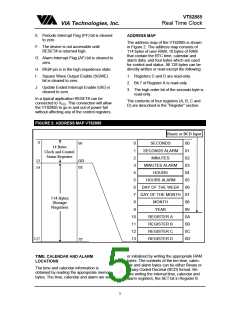
ADDRESS MAP
The address map of the VT82885 is shown
in Figure 2. The address map consists of
114 bytes of user RAM, 10 bytes of RAM
that contain the RTC time, calendar and
alarm data, and four bytes which are used
for control and status. All 128 bytes can be
directly written or read except the following:
F. The device is not accessible until
RESET# is returned high.
G. Alarm Interrupt Flag (AF) bit is cleared to
zero.
H. IRQ# pin is in the high impedence state.
I. Square Wave Output Enable (SQWE)
bit is cleared to zero.
1. Registers C and D are read-only.
2. Bit 7 of Register A is read-only.
J. Update Ended Interrupt Enable (UIE) is
cleared to zero.
3. The high order bit of the seconds byte is
read-only.
In a typical application RESET# can be
The contents of four registers (A, B, C and
D) are described in the “Register” section.
connected to V . This connection will allow
CC
the VT82885 to go in and out of power fail
without affecting any of the control registers.
FIGURE 2: ADDRESS MAP VT82885
Binary or BCD Input
0
00
0
1
SECONDS
SECONDS ALARM
MINUTES
00
01
02
03
04
05
14 Bytes
Clock and Control
Status Registers
2
13
14
OD
0E
3
MINUTES ALARM
HOURS
4
5
HOURS ALARM
6
DAY OF THE WEEK 06
DAY OF THE MONTH 07
7
114 Bytes
Storage
Registers
8
MONTH
YEAR
08
09
0A
0B
0C
0D
9
10
11
12
13
REGISTER A
REGISTER B
REGISTER C
REGISTER D
127
7F
or initialized by writing the appropriate RAM
bytes. The contents of the ten time, calen-
dar and alarm bytes can be either Binary or
Binary-Coded Decimal (BCD) format. Be-
fore writing the internal time, calendar and
alarm registers, the SET bit in Register B
TIME, CALENDAR AND ALARM
LOCATIONS
The time and calendar information is
obtained by reading the appropriate memory
bytes. The time, calendar and alarm are set
5

 ETC [ ETC ]