VT82885
Real Time Clock
VIA Technologies, Inc.
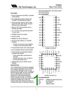
WR# (Write Strobe) − The WR# pin is used
to indicate a write cycle.
X1, X2 − These pins connect to a standard
32.768 kHz quartz crystal. The internal os-
cillator circuitry is designed for operation with
a crystal having a specified load capa-
citance (CL) of 6 pF. Each of the pins (X1
and X2) require the installation of an ex-
ternal 10 pF capacitor.
CS# (Chip Select Input) − The Chip Select
signal must be asserted low for a bus cycle
in the VT82885 to be accessed. CS# must
be kept in the active state during RD# and
WR#. Bus cycles which take place without
asserting CS# will latch addresses but no
RCLR# − The RCLR# pin is used to clear
(set to logic 1) all 114 bytes of general pur-
pose RAM but does not affect the RAM as-
sociated with the real time clock. In order to
clear the RAM, RCLR# must be forced to an
input logic of 0 (-0.3 to +0.8 volts) during
is below 4.25
access will occur. When V
CC
volts, the VT82885 internally inhibits access
cycles by internally disabling the CS# input.
This action protects both the real time clock
data and RAM data during power outages.
battery back-up mode when V is not ap-
CC
IRQ# (Interrupt Request Output) − The
IRQ# pin is an active low output of the
VT82885 that can be used as an interrupt
input to a processor. The IRQ# output
remains low as long as the status bit causing
the interrupt is present and the
plied. The RCLR# function is designed to be
used via human interface (shorting to ground
manually or by switch) and not to be driven
with external buffers. This pin is internally
pulled up.
corresponding interrupt-enable bit is set. To
clear the IRQ# pin the processor program
normally reads the C register. The RESET#
pin also clears pending interrupts.
AD0-AD7 (Multiplexed Bidirectional
Address/Data Bus) − Multiplexed buses
save pins because address information and
data information time share the same signal
paths. The addresses are present during the
first portion of the bus cycle and the same
pins and cycle paths are used for data in the
second portion of the cycle. Address/data
multiplexing does not slow the access time
of the VT82885 since the bus change from
address to data occurs during the internal
RAM access time. Addresses must be valid
prior to the falling edge of AS, at which time
the VT82885 latches the address from AD0
to AD6. Valid data must be present and held
stable during the latter portion of the RD# or
WR# pulses. In a read cycle the VT82885
outputs 8 bits of data during the latter portion
of the RD# or RD# pulses. The read cycle is
terminated and the bus returns to a high
impedence state as RD# transistions high as
in Intel timing.
When no interrupt condition is present, the
IRQ# level is in the high impedence state.
Multiple interrupting devices can be
connected to an IRQ# bus. The IRQ# bus is
an open drain output and requires an
external pull-up resistor.
RESET# (Reset Input) − The RESET# pin
has no effect on the clock, calendar, or
RAM. On power-up the RESET# pin can be
held low for a time in order to allow the
power supply to stabilize. The amount of
time that RESET# is held low is dependent
on the application. However, if RESET# is
used on power-up, the time RESET# is low
should exceed 200 ms to make sure that the
internal timer that controls the VT82885 on
power-up has timed out. When RESET# is
low and V is above 4.25 volts, the
CC
AS (Adress Strobe Input) − A positive
going address strobe pulse serves to
demultiplex the bus. The falling edge of AS
causes the address to be latched within the
VT82885.
following occurs:
A. Periodic Interrupt Enable (PEI) bit is
cleared to zero.
B. Alarm Interrupt Flag (AIE) bit is cleared
to zero.
RD# (Read Strobe) − The RD# pin identifies
the time period when the VT82885 drives the
bus with read data. The RD# signal is the
same definition as the Output Enable (OE#)
signal on a typical memory.
C. Update Ended Interrupt Flag (UF) bit is
cleared to zero.
D. Interrupt Request Status Flag (IRQF) bit
is cleared to zero.
4

 ETC [ ETC ]