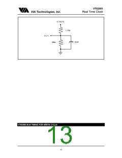
VT82885
Real Time Clock
VIA Technologies, Inc.
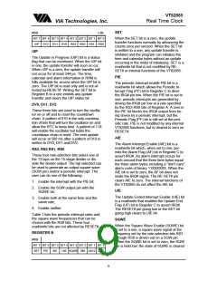
SET
MSB
LSB
BIT 7 BIT 6 BIT 5 BIT 4 BIT 3 BIT 2 BIT 1 BIT 0
UIP DV2 DV1 DV0 RS3 RS2 RS1 RS0
When the SET bit is a zero, the update
transfer functions normally by advancing the
counts once per second. When the SET bit
is written to a one, any update transfer is
inhibited and the program can initialize the
time and calendar bytes without an update
occurring in the midst of initializing. SET is a
read/write bit that is not modified by RE-
SET# or internal functions of the VT82885.
UIP
The Update in Progress (UIP) bit is a status
flag that can be monitored. When the UIP bit
is one, the update transfer will soon oc-cur.
When UIP is a zero, the update transfer will
not occur for at least 244 µs. The time,
calendar and alarm information in RAM is
fully available for access when the UIP bit is
zero. The UIP bit is read only and is not af-
fected by RESET#. Writing the SET bit in
Register B to a one inhibits any update
transfer and clears the UIP status bit.
PIE
The periodic interrupt enable PIE bit is a
read/write bit which allows the Periodic In-
terrupt Flag (PF) bit in Register C to drive
the IRQ# pin low. When the PIE bit is set to
one, periodic interrupts are generated by
driving the IRQ# pin low at a rate specified
by the RS3-RS0 bits of Register A. A zero in
the PIE bit blocks the IRQ# output from be-
ing driven by a periodic interrupt, but the
Periodic Flag (PF) bit is still set at the peri-
odic rate. PIE is not modified by any internal
VT82885 functions, but is cleared to zero on
RESET#.
DV0, DV1, DV2
These three bits are used to turn the oscilla-
tor on or off and to reset the countdown
chain. A pattern of 010 is the only combina-
tion of bits that will turn the oscillator on and
allow the RTC to keep time. A pattern of 11X
will enable the oscillator but holds the
countdown chain in reset. The next update
will occur at 500 ms after a pattern of 010 is
written to DV0, DV1 and DV2.
AIE
The Alarm Interrupt Enable (AIE) bit is a
read/write bit which, when set to one, per-
mits the Alarm Flag (AF) bit in Register C to
assert IRQ#. An alarm interrupt occurs for
each second that the three time bytes equal
the three alarm bytes including a “don’t care”
alarm code of binary 11XXXXXX. When the
AIE bit is set to zero, the AF bit does not
iniate the IRQ# signal. The RE-SET# pin
clears AIE to zero. The internal functions of
the VT82885 do not affect the AIE bit.
RS3, RS2 RS1, RS0
These four rate-selection bits select one of
the 13 taps on the 15-stage divider or dis-
able the divider output. The tap selected can
be used to generate an output square wave
(SQW pin) and/or a periodic interrupt. The
user can do one of the following:
1. Enable the interrupt with the PIE bit;
2. Enable the SQW output pin with the
SQWE bit;
UIE
The Update Ended Interrupt Enable (UIE) bit
is a read/write that enables the Update End
Flag (UF) bit in Register C to assert IRQ#.
The RESET# pin going low or the SET bit
going high clears to UIE bit.
3. Enable both at the same time and the
same rate;
4. Enable neither.
Table 1 lists the periodic interrupt rates and
the square wave frequencies that can be
chosen with the RS# bits. These four
SQWE
When the Square Wave Enable (SQWE) bit
is set to a one, a square wave signal at the
frequency set by the rate-selection bits RS3
through RS0 is driven out on a SQW pin.
When the SQWE bit is set to zero, the SQW
pin is held low; the state of SQWE is cleared
read/write bits are not affected by RESET#.
REGISTER B
MSB
BIT 7 BIT 6 BIT 5 BIT 4 BIT 3 BIT 2 BIT 1 BIT 0
SET PIE AIE UIE SQWE DM 24/12 DSE
LSB
9

 ETC [ ETC ]