VT82885
Real Time Clock
VIA Technologies, Inc.
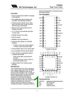
WR#
- Write Strobe
GND
- Ground
RD#
RESET#
IRQ#
- Read Strobe
- Reset Input
- Interrupt Request Output
- Square Wave Output
- +5 Volt Supply
X1, X2
- 32.768 kHz Crystal Connec-
tions
- +3 Volt Battery Input
- RAM Clear
V
BAT
#
SQW
RCLR#
V
CC
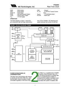
OPERATION
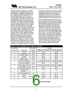
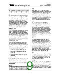
The block diagram in Figure 1 shows the
pin connections with the major internal func-
tions of the VT82885. The following para-
graphs describe the function of each pin.
FIQURE 1: BLOCK DIAGRAM VT82885
X1
OSC
X2
+8
+64
+64
CS#
POWER
SWITCH
AND
PERIODIC INTERUPT SQUARE WAVE
SELECTOR
VCC
VCC
WRITE
PROTECT
POK
VBAT
SQUARE
WAVE OUT
SQW
CS#
IRQ#
RESET#
REGISTERS A,B,C,D
RD#
WR#
AS
CLOCK/
CALENDAR
UPDATE
CLOCK, CALENDAR
AND ALARM RAM
BUS
INTERFACE
AD0-
AD7
BCD/
BINARY
INCREMENT
USER RAM
114 BYTES
RCLR#
GND
input. When V is applied to the VT82885
CC
POWER-DOWN/POWER-UP
CONSIDERATIONS
and reaches a level of greater than 4.25
volts, the device becomes ac-cessible after
100 ms, provided that the oscillator is
running and the oscillator countdown chain
is not in reset (see Register A). This time
period allows the system to stabilize after
The Real Time Clock function will continue
to operate and all of the RAM, time, calen-
dar and alarm memory locations remain
nonvolatile regardless of the level of the V
CC
2

 ETC [ ETC ]