iW1688
Low-Power Off-line Digital PWM Controller
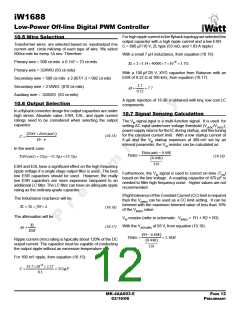
For high ripple current in the flyback topology we selected the
output capacitor with a high ripple current and a low ESR.
C = 680 µF/10 V, ZL type (53 mΩ, and 1.03 A ripple)
10.5 Wire Selection
Transformer wires are selected based on input/output rms
current and circle.mil/amp of each type of wire. We select
500cir.mils for every 1A rms. Therefore:
With a small 7 µH inductance, from equation (10.16):
XL = 2×3.14× 40000× 7×10−6 =1.7Ω
Primary wire = 500 cir.mils x 0.147 = 73 cir.mils
Primary wire = 32AWG (63 cir.mils)
With a 100 µF/25 V, XYG capacitor from Rubycon with an
ESR of 0.22 Ω at 100 kHz, from equation (10.17):
Secondary wire = 500 cir.mils x 2.857/1.3 = 992 cir.mils
Secondary wire = 21AWG (810 cir.mils)
Auxiliary wire = 32AWG (63 cir.mils)
1.7
AR =
= 7.7
0.22
A ripple rejection of 18 dB is obtained with tiny, low cost LC
components.
10.6 Output Selection
In a flyback converter design the output capacitors are under
high stress. Absolute value, ESR, ESL, and ripple current
ratings need to be considered when selecting the output
capacitor.
10.7 Signal Sensing Calculation
The VIN signal input is a multi-function signal. It is used for
setting AC input under/over voltage threshold (VUVDC/VOVDC),
power supply source for the IC during startup, and fine tuning
for the constant current limit. With a low startup current of
8 μA and the VIN startup maximum at 488 mV set by an
internal parameter, the VIN resistor can be calculated as:
TOFF × IOUT (MAX )
(
)
(10.15)
C =
VP − P
In the worst case:
TOFF(MAX ) = 25µs −11.3µs =13.7µs
VINDC(MIN) − 0.448
VINRES =
(10.18)
0.448
(
)
25k
ESR and ESL have a significant effect on the high frequency
ripple voltage if a single stage output filter is used. The best
low ESR capacitors should be used. However, the really
low ESR capacitors are more expensive compared to an
additional LC filter. The LC filter can have an adequate ripple
rating as the ordinary-grade capacitor.
Furthermore, the VIN signal is used to correct on-time (TON)
based on the line voltage. A coupling capacitor of 470 pF is
needed to filter high frequency noise. Higher values are not
recommended.
If tight tolerance of the Constant Current (CC) limit is required
then the VINRES can be used as a CC limit setting. It can be
trimmed with the maximum trimmed value of less than 10%
of the VINRES value.
The Inductance reactance will be:
XL = 2π × fSW × L
(10.16)
(10.17)
The attenuation will be:
VIN resistor (refer to schematic: VINRES = R1 + R2 + R3)
With the VINDC(MIN) of 93 V, from equation (10.18):
93 − 0.448
XL
AR =
ESR
(
)
= 5.16M
VINRES =
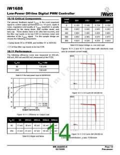
Ripple current (rms) rating is typically about 120% of the DC
output current. The capacitor must be capable of conducting
the output ripple without an excessive temperature rise.
0.448
(
)
25k
For 100 mV ripple, from equation (10.15):
13.7×10−6 × 2.57
C =
= 352µF
0.1
MK-4AA003-E
03/16/06
PAGE 12
PRELIMINARY

 ETC [ ETC ]