iW1688
Low-Power Off-line Digital PWM Controller
The primary feedback signal from the auxiliary winding will
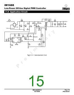
10.8 Component Values
reveal the secondary voltage at a different load. Short circuit
and over voltage supply power to the system after starting
up. From figure 9.6.1, VAUX corner (right before voltage starts
falling) is the information that the system will read cycle by
cycle to generate a feedback voltage (VFB). The VFB precisely
represents the output voltage and is used to regulate the
output voltage by changing TON/TOFF. Pay close attention to
this corner signal condition. To avoid any unwanted stray
signals at that corner, the follow things need to be done:
Component
LM
Value
2.5 mH
N
16.7
NSEC
12 turns
200 turns
30 turns
3 A/40 V
28 AWG
17.87 kΩ
2.21 kΩ
2.4 MΩ
NPR
NAUX
1. The bias rectifier diode has to be a fast recovery diode
(50ns or lower) to prevent reverse voltage from the bias
voltage source.
Diode, D9
Secondary Wire
RSENSEIN
RSENSE
R1, R2
R3
2. The bias capacitor must be low ESR to minimize ripple &
noise at VCC. For example: YK type from Rubycon
3. The distance from the transformer to VSENSE should be as
short as possible to minimize the parasitic signal.
4. The impedance between VSENSE and the transformer is
(RSENSEIN) about 20 kΩ to minimize the signal’s sensitivity.
VSENSE is typically 1.54 V:
1.2 MΩ
C1, C2
4.7 µF/400 V
1.54
RSENSE =
Table10.3 Final component values based on actual circuitry
VAUX −1.54
(
)
(10.19)
20k
10.9 PCB Layout
Due to the limited ranges of the resistor, a trim resistor or
a parallel resistor is needed to set the output voltage to the
desired limit.
A switch mode power supply layout has various separate
grounds in the PCB such as the power ground, switching
ground, and control logic ground. They all need to keep
in short distance and end up at one point at the power
ground. The trace for the switching ground is thick to lower
switching loss. Power ground must be as thick as ground
plane possible. This technique will help to reduce EMI and
ripple noise. It is recommended that the trace that connects
the transformer to the VSENSE pin is as short as possible to
improve the VSENSE signal quality as mentioned in the signal
sensing calculation section.
With VAUX = 13 V, from equation (10.19):
1.54
13 −1.54
RSENSE =
= 2.78k
(
)
20k
The VCC pin is the input power supply for iW1688 after startup.
Due to the sensitive internal circuitry an extra RC filter is
needed to filter rejection noise. The recommend values of
the RC filter are 100 Ω and 0.47 µF ceramic capacitor (type
X7R) in parallel with a 2.2 µF/25V electrolytic capacitor.
MK-4AA003-E
03/16/06
PAGE 13
PRELIMINARY

 ETC [ ETC ]