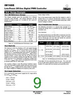
iW1688
Low-Power Off-line Digital PWM Controller
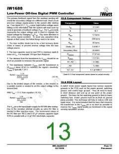
10.10 Critical Components
Load
90V
115V
230V
264V
(mA)
The primary feedback signal VSENSE is the most important
signal to control output performance (i.e. VI curve, ripple &
noise, regulation) and quality of VSENSE waveform is greatly
influenced by the clamp diode, bias rectifier diode, and
bias cap. These diodes have to be ultra fast recovery, and
the filter cap needs to be low ESR to minimize noise and
distortion of the VSENSE signal. For this sample design we
choose the following components:
0
5.14V
5.04V
5.00V
4.96V
4.93V
5.14V
5.04V
5.00V
4.96V
4.93V
5.13V
5.04V
5.00V
4.97V
4.93V
5.13V
5.34V
5.00V
4.97V
4.93V
200
400
600
800
• Clamp diode D5 is UF4006, and rectifier D1 is HER102
• C7 of Bias filter cap needs to be low ESR.
Table10.6 Output Voltage vs. Line and Load
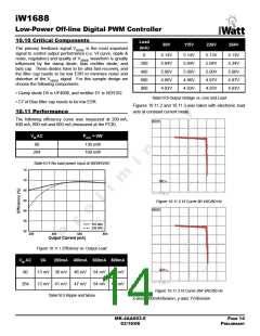
Figures 10.11.2 and 10.11.3 was taken with electronic load
sets at constant current mode.
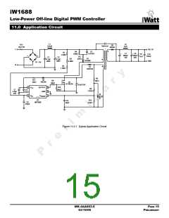
10.11 Performance
The following efficiency curve was measured at 200 mA,
400 mA, 600 mA and 800 mA (measured at the PCB).
VIN AC
POUT = 0W
90
130 mW
160 mW
264
Table10.4 No load power input at 90/264VAC
74
70
66
64
60
56
52
Figure 10.11.2 VI Curve 90 VAC/60 Hz
115 VAC
230 VAC
200
400
600
800
Output Current (mA)
Figure 10.11.1 Efficiency vs. Output Load
VIN AC
90
0A
200mA 400mA 600mA 800mA
13 mV 38 mV
13 mV 41 mV
46 mV
47 mV
54 mV 60 mV
54 mV 63 mV
264
Figure 10.11.3 VI Curve 264 VAC/50 Hz
Table10.5 Ripple and Noise
x-axis: 200mA/division, y-axis:1V/division
MK-4AA003-E
03/16/06
PAGE 14
PRELIMINARY

 ETC [ ETC ]