a-Si TFT LCD Single Chip Driver
240RGBx320 Resolution and 262K color
ILI9325
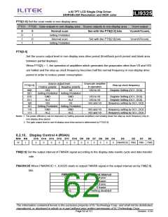
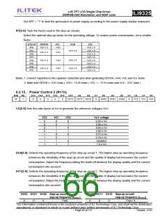
PTG[1:0] Set the scan mode in non-display area.
PTG1 PTG0 Gate outputs in non-display area Source outputs in non-display area
Vcom output
0
0
Normal scan
Set with the PTS[2:0] bits
VcomH/VcomL
0
1
-
-
Setting Prohibited
Interval scan
1
1
0
1
Set with the PTS[2:0] bits
-
VcomH/VcomL
-
Setting Prohibited
PTS[2:0]
Set the source output level in non-display area drive period (front/back porch period and blank area
between partial displays).
When PTS[2] = 1, the operation of amplifiers which generates the grayscales other than V0 and V63
are halted and the step-up clock frequency becomes half the normal frequency in non-display drive
period in order to reduce power consumption.
Source output level
Grayscale amplifier
in operation
V63 to V0
-
PTS[2:0]
Step-up clock frequency
Positive polarity
V63
Negative polarity
V0
000
001
010
011
100
101
110
111
Register Setting (DC1, DC0)
-
Setting Prohibited Setting Prohibited
GND
Hi-Z
V63
GND
Hi-Z
V0
V63 to V0
V63 to V0
V63 and V0
-
Register Setting (DC1, DC0)
Register Setting (DC1, DC0)
frequency setting by DC1, DC0
-
Setting Prohibited Setting Prohibited
GND
Hi-Z
GND
Hi-Z
V63 and V0
V63 and V0
frequency setting by DC1, DC0
frequency setting by DC1, DC0
Notes: 1. The power efficiency can be improved by halting grayscale amplifiers and slowing down the step-up clock frequency only in
non-display drive period.
2. The gate output level in non-lit display area drive period is determined by PTG[1:0].
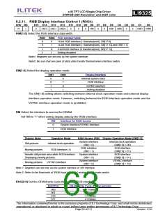
8.2.10. Display Control 4 (R0Ah)
R/W RS
D15 D14 D13 D12 D11 D10 D9 D8 D7 D6 D5 D4
D3
D2
D1
D0
W
1
0
0
0
0
0
0
0
0
0
0
0
0
FMARKOE FMI2 FMI1 FMI0
FMI[2:0] Set the output interval of FMARK signal according to the display data rewrite cycle and data transfer
rate.
FMARKOE When FMARKOE=1, ILI9325 starts to output FMARK signal in the output interval set by FMI[2:0]
bits.
FMI[2:0]
000
Output Interval
1 frame
001
2 frame
011
4 frame
101
6 frame
Others
Setting disabled
The information contained herein is the exclusive property of ILI Technology Corp. and shall not be distributed,
reproduced, or disclosed in whole or in part without prior written permission of ILI Technology Corp.
Page 62 of 111
Version: 0.35

 ETC [ ETC ]