Data Sheet
June 1999
ORCA Series 2 FPGAs
transition of a clock or latch enable signal, during
which the data must be stable to ensure it is recog-
nized as the intended value.
ORCA Timing Characteristics
(continued)
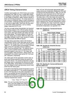
Table 15B. Derating for Commercial/Industrial
Devices (OR2TxxB)
■ Hold Time—the interval immediately following the
transition of a clock or latch enable signal, during
which the data must be held stable to ensure it is rec-
ognized as the intended value.
Power Supply Voltage
TJ
(°C)
3.0 V
3.15 V
3.3 V
3.45 V
3.6 V
–40
0
25
85
100
125
0.81
0.86
0.9
1.0
1.02
1.06
0.78
0.83
0.87
0.95
0.98
1.03
0.76
0.80
0.83
0.93
0.95
0.98
0.74
0.77
0.8
0.88
0.91
0.95
0.73
0.76
0.78
0.86
0.88
0.92
■ 3-state Enable—the time from when a TS[3:0] signal
becomes active and the output pad reaches the high-
impedance state.
Estimating Power Dissipation
Note: The derating tables shown above are for a typical critical path
that contains 33% logic delay and 66% routing delay. Since the
routing delay derates at a higher rate than the logic delay, paths
with more than 66% routing delay will derate at a higher rate
than shown in the table. The approximate derating values vs.
temperature are 0.26% per °C for logic delay and 0.45% per °C
for routing delay. The approximate derating values vs. voltage
are 0.13% per mV for both logic and routing delays at 25 °C.
OR2CxxA
The total operating power dissipated is estimated by
summing the standby (IDDSB), internal, and external
power dissipated. The internal and external power is
the power consumed in the PLCs and PICs, respec-
tively. In general, the standby power is small and may
be neglected. The total operating power is as follows:
In addition to supply voltage, process variation, and
operating temperature, circuit and process improve-
ments of the ORCA series FPGAs over time will result
in significant improvement of the actual performance
over those listed for a speed grade. Even though lower
speed grades may still be available, the distribution of
yield to timing parameters may be several speed bins
higher than that designated on a product brand. Design
practices need to consider best-case timing parame-
ters (e.g., delays = 0), as well as worst-case timing.
PT = Σ PPLC + Σ PPIC
The internal operating power is made up of two parts:
clock generation and PFU output power. The PFU out-
put power can be estimated based upon the number of
PFU outputs switching when driving an average fan-out
of two:
PPFU = 0.16 mW/MHz
For each PFU output that switches, 0.16 mW/MHz
needs to be multiplied times the frequency (in MHz)
that the output switches. Generally, this can be esti-
mated by using one-half the clock rate, multiplied by
some activity factor; for example, 20%.
The routing delays are a function of fan-out and the
capacitance associated with the CIPs and metal inter-
connect in the path. The number of logic elements that
can be driven (or fan-out) by PFUs is unlimited,
although the delay to reach a valid logic level can
exceed timing requirements. It is difficult to make accu-
rate routing delay estimates prior to design compilation
based on fan-out. This is because the CAE software
may delete redundant logic inserted by the designer to
reduce fan-out, and/or it may also automatically reduce
fan-out by net splitting.
The power dissipated by the clock generation circuitry
is based upon four parts: the fixed clock power, the
power/clock branch row or column, the clock power dis-
sipated in each PFU that uses this particular clock, and
the power from the subset of those PFUs that is config-
ured in either of the two synchronous modes (SSPM or
SDPM). Therefore, the clock power can be calculated
for the four parts using the following equations:
The waveform test points are given in the Measure-
ment Conditions section of this data sheet. The timing
parameters given in the electrical characteristics tables
in this data sheet follow industry practices, and the val-
ues they reflect are described below.
OR2C04A Clock Power
P
= [0.62 mW/MHz
+ (0.22 mW/MHz – Branch) (# Branches)
+ (0.022 mW/MHz – PFU) (# PFUs)
+ (0.006 mW/MHz – SMEM_PFU)
(# SMEM_PFUs)] fCLK
■ Propagation Delay—the time between the specified
reference points. The delays provided are the worst
case of the tphh and tpll delays for noninverting func-
tions, tplh and tphl for inverting functions, and tphz
and tplz for 3-state enable.
For a quick estimate, the worst-case (typical circuit)
OR2C04A clock power ≈ 3.9 mW/MHz.
■ Setup Time—the interval immediately preceding the
Lucent Technologies Inc.
61

 ETC [ ETC ]