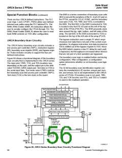
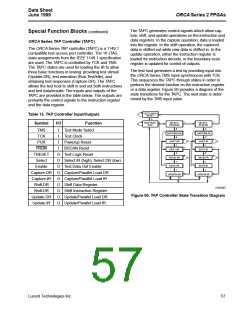
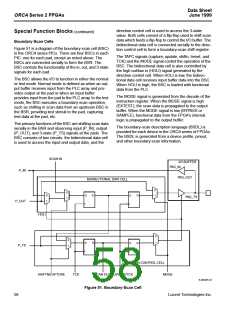
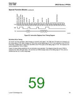
Data Sheet
June 1999
ORCA Series 2 FPGAs
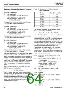
Table 14A and 14B and provide approximate power
ORCA Timing Characteristics
supply and junction temperature derating for OR2CxxA
commercial and industrial devices. Table 15A and 15B
provides the same information for the OR2TxxA and
OR2TxxB devices (both commercial and industrial).
The delay values in this data sheet and reported by
ORCA Foundry are shown as 1.00 in the tables. The
method for determining the maximum junction temper-
ature is defined in the Thermal Characteristics section.
Taken cumulatively, the range of parameter values for
best-case vs. worst-case processing, supply voltage,
and junction temperature can approach 3 to 1.
To define speed grades, the ORCA Series part number
designation (see Table 54) uses a single-digit number
to designate a speed grade. This number is not related
to any single ac parameter. Higher numbers indicate a
faster set of timing parameters. The actual speed sort-
ing is based on testing the delay in a path consisting of
an input buffer, combinatorial delay through all PLCs in
a row, and an output buffer. Other tests are then done
to verify other delay parameters, such as routing
delays, setup times to FFs, etc.
The most accurate timing characteristics are reported
by the timing analyzer in the ORCA Foundry Develop-
ment System. A timing report provided by the develop-
ment system after layout divides path delays into logic
and routing delays. The timing analyzer can also pro-
vide logic delays prior to layout. While this allows rout-
ing budget estimates, there is wide variance in routing
delays associated with different layouts.
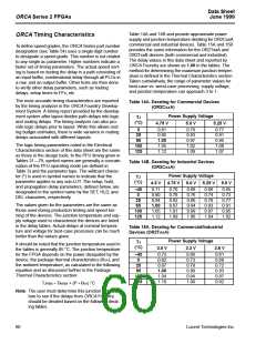
Table 14A. Derating for Commercial Devices
(OR2CxxA)
Power Supply Voltage
TJ
(°C)
4.75 V
5.0 V
5.25 V
0
25
85
100
125
0.81
0.85
1.00
1.05
1.12
0.79
0.83
0.97
1.02
1.09
0.77
0.81
0.95
1.00
1.07
The logic timing parameters noted in the Electrical
Characteristics section of this data sheet are the same
as those in the design tools. In the PFU timing given in
Tables 31—79, symbol names are generally a concate-
nation of the PFU operating mode (as defined in
Table 3) and the parameter type. The wildcard charac-
ter (*) is used in symbol names to indicate that the
parameter applies to any sub-LUT. The setup, hold,
and propagation delay parameters, defined below, are
designated in the symbol name by the SET, HLD, and
DEL characters, respectively.
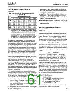
Table 14B. Derating for Industrial Devices
(OR2CxxA)
Power Supply Voltage
TJ
(°C)
4.5 V 4.75 V 5.0 V 5.25 V 5.5 V
–40
0
25
85
100
125
0.71
0.80
0.84
1.00
1.05
1.12
0.70
0.78
0.82
0.97
1.01
1.09
0.68
0.76
0.80
0.94
0.99
1.06
0.66
0.74
0.78
0.93
0.97
1.04
0.65
0.73
0.77
0.91
0.95
1.02
The values given for the parameters are the same as
those used during production testing and speed bin-
ning of the devices. The junction temperature and sup-
ply voltage used to characterize the devices are listed
in the delay tables. Actual delays at nominal tempera-
ture and voltage for best-case processes can be much
better than the values given.
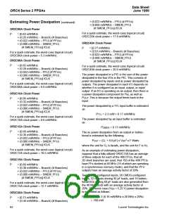
Table 15A. Derating for Commercial/Industrial
Devices (OR2TxxA)
Power Supply Voltage
3.3 V
TJ
(°C)
It should be noted that the junction temperature used in
the tables is generally 85 °C. The junction temperature
for the FPGA depends on the power dissipated by the
device, the package thermal characteristics (ΘJA), and
the ambient temperature, as calculated in the following
equation and as discussed further in the Package
Thermal Characteristics section:
3.0 V
3.6 V
–40
0
25
85
100
125
0.73
0.82
0.87
1.00
1.04
1.10
0.66
0.73
0.78
0.90
0.94
1.00
0.61
0.68
0.72
0.83
0.87
0.92
TJmax = TAmax + (P • ΘJA) °C
Note: The user must determine this junction tempera-
ture to see if the delays from ORCA Foundry
should be derated based on the following derat-
ing tables.
60
Lucent Technologies Inc.

 ETC [ ETC ]