Data Sheet
June 1999
ORCA Series 2 FPGAs
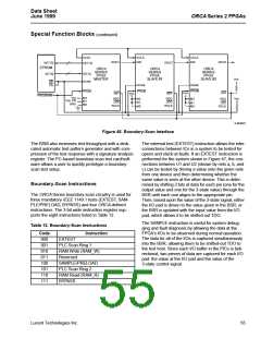
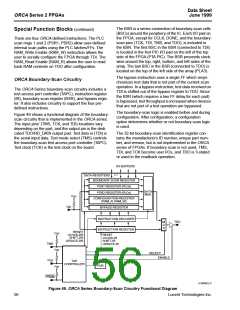
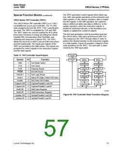
Special Function Blocks (continued)
TCK
TMS
TDI
Fig.5.3(F)
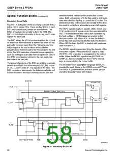
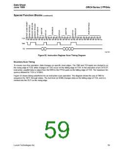
Figure 52. Instruction Register Scan Timing Diagram
Boundary-Scan Timing
To ensure race-free operation, data changes on specific clock edges. The TMS and TDI inputs are clocked in on
the rising edge of TCK, while changes on TDO occur on the falling edge of TCK. In the execution of an EXTEST
instruction, parallel data is output from the BSR to the FPGA pads on the falling edge of TCK. The maximum fre-
quency allowed for TCK is 10 MHz.
Figure 52 shows timing waveforms for an instruction scan operation. The diagram shows the use of TMS to
sequence the TAPC through states. The test host (or BSM) changes data on the falling edge of TCK, and it is
clocked into the DUT on the rising edge.
Lucent Technologies Inc.
59

 ETC [ ETC ]