Data Sheet
June 1999
ORCA Series 2 FPGAs
power dissipated by inputs and ac power dissipated by
outputs. The power dissipated in each I/O depends on
whether it is configured as an input, output, or input/
output. If an I/O is operating as an output, then there is
a power dissipation component for PIN, as well as
POUT. This is because the output feeds back to the
input.
Estimating Power Dissipation (continued)
OR2T15B and OR2T40B
The total operating power dissipated is estimated by
summing the standby (IDDSB), internal, and external
power dissipated. The internal and external power is
the power consumed in the PLCs and PICs, respec-
tively. In general, the standby power is small and may
be neglected. The total operating power is as follows:
The power dissipated by an input buffer (VIH = VDD –
0.3 V or higher) is estimated as:
PIN = 0.033 mW/MHz
PT = Σ PPLC + Σ PPIC
The OR2TxxB 5 V tolerant input buffer feature does not
dissipate additional dc power.
The internal operating power is made up of two parts:
clock generation and PFU output power. The PFU out-
put power can be estimated based upon the number of
PFU outputs switching when driving an average fan-out
of two:
The ac power dissipation from an output or bidirec-
tional is estimated by the following:
2
POUT = (CL + 8.8 pF) x VDD x F Watts
PPFU = 0.08 mW/MHz
where the unit for CL is farads, and the unit for F is Hz.
For each PFU output that switches, 0.08 mW/MHz
needs to be multiplied times the frequency (in MHz)
that the output switches. Generally, this can be esti-
mated by using one-half the clock rate, multiplied by
some activity factor; for example, 20%.
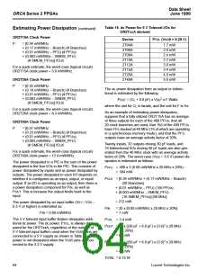
As an example of estimating power dissipation,
suppose that a fully utilized OR2T15B has an average
of three outputs for each of the 400 PFUs, that all
20 clock branches are used, that 150 of the 400 PFUs
have FFs clocked at 40 MHz (16 of which are operating
in a synchronous memory mode), and that the PFU
outputs have an average activity factor of 20%.
The power dissipated by the clock generation circuitry
is based upon four parts: the fixed clock power, the
power/clock branch row or column, the clock power dis-
sipated in each PFU that uses this particular clock, and
the power from the subset of those PFUs that is config-
ured in either of the two synchronous modes (SSPM or
SDPM). Therefore, the clock power can be calculated
for the four parts using the following equations:
Twenty inputs, 32 outputs driving 30 pF loads, and
16 bidirectional I/Os driving 50 pF loads are also gen-
erated from the 40 MHz clock with an average activity
factor of 20%. The worst-case (VDD = 3.6 V) power dis-
sipation is estimated as follows:
PPFU = 400 x 3 (0.08 mW/MHz x 20 MHz x 20%)
= 384 mW
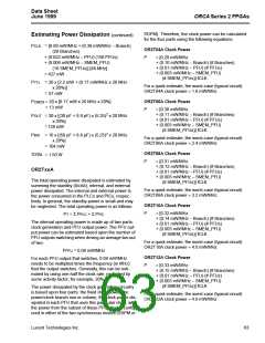
OR2T15B Clock Power
PCLK = [0.30 mW/MHz + (0.085 mW/MHz – Branch)
(20 Branches)
P
= [0.30 mW/MHz
+ (0.85 mW/MHz – Branch) (# Branches)
+ (0.008 mW/MHz – PFU) (# PFUs)
+ (0.002 mW/MHz – SMEM_PFU)
(# SMEM_PFUs)] fCLK
+ (0.008 mW/MHz – PFU) (150 PFUs)
+ (0.002 mW/MHz – SMEM_PFU)
(16 SMEM_PFUs)] [40 MHz]
= 129 mW
For a quick estimate, the worst-case (typical circuit)
OR2T15B clock power ≈ 3.9 mW/MHz.
PIN
= 20 x [0.033 mW/MHz x 20 MHz x 20%]
= 3 mW
OR2T40B Clock Power
PTOL = 3.4 mW
P
= [0.42 mW/MHz
POUT = 30 x [(30 pF + 8.8 pF) x (3.6)2 x 20 MHz
+ (0.118 mW/MHz – Branch) (# Branches)
+ (0.008 mW/MHz – PFU) (# PFUs)
+ (0.002 mW/MHz – SMEM_PFU)
(# SMEM_PFUs)] fCLK
x 20%]
= 60 mW
PBID = 16 x [(50 pF + 8.8 pF) x (3.6)2 x 20 MHz
For a quick estimate, the worst-case (typical circuit)
OR2T40B clock power ≈ 5.5 mW/MHz.
x 20%]
= 49 mW
The power dissipated in a PIC is the sum of the power
dissipated in the four I/Os in the PIC. This consists of
TOTAL = 0.72 W
Lucent Technologies Inc.
65

 ETC [ ETC ]