Data Sheet
June 1999
ORCA Series 2 FPGAs
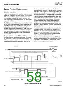
The BSR is a series connection of boundary-scan cells
(BSCs) around the periphery of the IC. Each I/O pad on
the FPGA, except for CCLK, DONE, and the boundary-
scan pins (TCK, TDI, TMS, and TDO), is included in
the BSR. The first BSC in the BSR (connected to TDI)
is located in the first PIC I/O pad on the left of the top
side of the FPGA (PTA PIC). The BSR proceeds clock-
wise around the top, right, bottom, and left sides of the
array. The last BSC in the BSR (connected to TDO) is
located on the top of the left side of the array (PLA3).
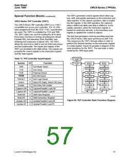
Special Function Blocks (continued)
There are four ORCA-defined instructions. The PLC
scan rings 1 and 2 (PSR1, PSR2) allow user-defined
internal scan paths using the PLC latches/FFs. The
RAM_Write Enable (RAM_W) instruction allows the
user to serially configure the FPGA through TDI. The
RAM_Read Enable (RAM_R) allows the user to read
back RAM contents on TDO after configuration.
The bypass instruction uses a single FF which resyn-
chronizes test data that is not part of the current scan
operation. In a bypass instruction, test data received on
TDI is shifted out of the bypass register to TDO. Since
the BSR (which requires a two FF delay for each pad)
is bypassed, test throughput is increased when devices
that are not part of a test operation are bypassed.
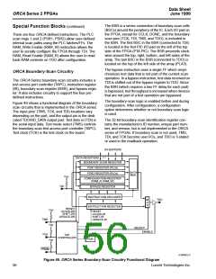
ORCA Boundary-Scan Circuitry
The ORCA Series boundary-scan circuitry includes a
test access port controller (TAPC), instruction register
(IR), boundary-scan register (BSR), and bypass regis-
ter. It also includes circuitry to support the four pre-
defined instructions.
The boundary-scan logic is enabled before and during
configuration. After configuration, a configuration
option determines whether or not boundary-scan logic
is used.
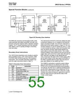
Figure 49 shows a functional diagram of the boundary-
scan circuitry that is implemented in the ORCA series.
The input pins’ (TMS, TCK, and TDI) locations vary
depending on the part, and the output pin is the dedi-
cated TDO/RD_DATA output pad. Test data in (TDI) is
the serial input data. Test mode select (TMS) controls
the boundary-scan test access port controller (TAPC).
Test clock (TCK) is the test clock on the board.
The 32-bit boundary-scan identification register con-
tains the manufacturer’s ID number, unique part num-
ber, and version, but is not implemented in the ORCA
series of FPGAs. If boundary scan is not used, TMS,
TDI, and TCK become user I/Os, and TDO is 3-stated
or used in the readback operation.
I/O BUFFERS
DATA REGISTERS
BOUNDARY-SCAN REGISTER
PSR1 REGISTER (PLCs)
PSR2 REGISTER (PLCs)
DATA
MUX
V
DD
CONFIGURATION REGISTER
(RAM_R, RAM_W)
TDI
BYPASS REGISTER
INSTRUCTION DECODER
INSTRUCTION REGISTER
TDO
M
U
X
RESET
V
V
V
DD
DD
DD
CLOCK-DR
SHIFT-DR
RESET
CLOCK-IR
SHIFT-IR
UPDATE-IR
UPDATE-DR
TMS
TCK
SELECT
ENABLE
TAP
CONTROLLER
PUR
PRGM
5-2840(C).r7
Figure 49. ORCA Series Boundary-Scan Circuitry Functional Diagram
Lucent Technologies Inc.
56

 ETC [ ETC ]