Data Sheet
June 1999
ORCA Series 2 FPGAs
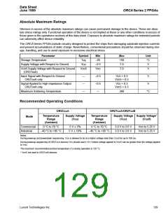
Absolute Maximum Ratings
Stresses in excess of the absolute maximum ratings can cause permanent damage to the device. These are abso-
lute stress ratings only. Functional operation of the device is not implied at these or any other conditions in excess of
those given in the operations sections of this data sheet. Exposure to absolute maximum ratings for extended periods
can adversely affect device reliability.
The ORCA Series FPGAs include circuitry designed to protect the chips from damaging substrate injection currents
and prevent accumulations of static charge. Nevertheless, conventional precautions should be observed during stor-
age, handling, and use to avoid exposure to excessive electrical stress.
Parameter
Storage Temperature
Symbol
Tstg
Min
–65
–0.5
VDD
Max
150
7.0
Unit
°C
V
Supply Voltage with Respect to Ground
VDD
VDD5 Supply Voltage with Respect to Ground
(OR2TxxA)
VDD5
7.0
V
Input Signal with Respect to Ground
OR2TxxA only
—
—
—
–0.5
–0.5
—
VDD + 0.3
VDD5 + 0.3
V
V
Signal Applied to High-impedance Output
OR2TxxA only
VDD + 0.3
VDD5 + 0.3
Maximum Soldering Temperature
260
°C
Recommended Operating Conditions
OR2CxxA
OR2TxxA/OR2TxxB
Temperature
Range
Supply Voltage
(VDD)
Temperature
Range
Supply Voltage Supply Voltage*
Mode
(VDD)
(VDD5)
(Ambient)
(Ambient)
Commercial
Industrial
Notes:
0 °C to 70 °C
5 V ± 5%
0 °C to 70 °C
3.0 V to 3.6 V
3.0 V to 3.6 V
VDD to 5.25 V
VDD to 5.25 V
–40 °C to +85 °C
5 V ± 10%
–40 °C to +85 °C
During powerup and powerdown sequencing, VDD is allowed to be at a higher voltage level than VDD5 for up to 100 ms.
During powerup sequencing of OR2TxxA devices VDD should reach 1.0 V before voltage applied to VDD5 can be greater than the voltage applied
to VDD.
The maximum recommended junction temperature (TJ) during operation is 125 °C.
* VDD5 not used in OR2TxxB devices.
Lucent Technologies Inc.
129

 ETC [ ETC ]