Data Sheet
June 1999
ORCA Series 2 FPGAs
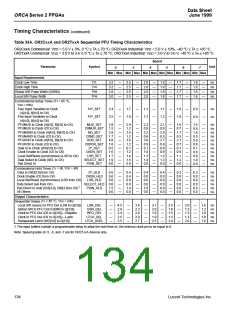
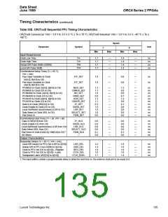
Timing Characteristics
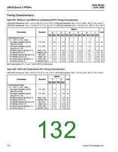
Table 32A. OR2CxxA and OR2TxxA Combinatorial PFU Timing Characteristics
OR2CxxA Commercial: VDD = 5.0 V ± 5%, 0 °C ≤ TA ≤ 70 °C; OR2CxxA Industrial: VDD = 5.0 V ± 10%, –40 °C ≤ TA ≤ +85 °C.
OR2TxxA Commercial: VDD = 3.0 V to 3.6 V, 0 °C ≤ TA ≤ 70 °C; OR2TxxA Industrial: VDD = 3.0 V to 3.6 V, –40 °C ≤ TA ≤ +85 °C.
Speed
Unit
Parameter
Symbol
-2
-3
-4
-5
-6
-7
Min Max Min Max Min Max Min Max Min Max Min Max
Combinatorial Delays
(TJ = +85 °C, VDD = min):
Four Input Variables (A[4:0],
B[4:0] to F[3:0])
Five Input Variables (A[4:0],
B[4:0] to F3, F0)
F4*_DEL
F5*_DEL
—
—
4.0
4.1
—
—
2.8
2.9
—
—
2.1
2.2
—
—
1.7
1.8
—
—
1.4
1.4
—
—
1.3 ns
1.3 ns
PFUMUX (A[4:0], B[4:0] to F1)
PFUMUX (C0 to f1)
PFUNAND (A[4:0], B[4:0] to F2)
PFUNAND (C0 to F2)
PFUXOR (A[4:0], B[4:0] to F1)
PFUXOR (C0 to F1)
MUX_DEL
C0MUX_DEL
ND_DEL
C0ND_DEL
XOR_DEL
—
—
—
—
—
—
4.7
3.0
4.7
2.7
5.6
3.1
—
—
—
—
—
—
3.8
2.2
4.0
2.2
4.5
2.2
—
—
—
—
—
—
3.2
1.9
3.3
1.8
3.8
2.0
—
—
—
—
—
—
2.6
1.5
2.7
1.5
3.1
1.6
—
—
—
—
—
—
1.9
1.1
1.8
1.0
2.3
1.1
—
—
—
—
—
—
1.8 ns
1.0 ns
1.7 ns
0.8 ns
2.1 ns
1.0 ns
C0XOR_DEL
Note: Speed grades of -5, -6, and -7 are for OR2TxxA devices only.
Table 32B. OR2TxxB Combinatorial PFU Timing Characteristics
OR2TxxB Commercial: VDD = 3.0 V to 3.6 V, 0 °C ≤ TA ≤ 70 °C; OR2TxxB Industrial: VDD = 3.0 V to 3.6 V, –40 °C ≤ TA ≤ +85°C.
Speed
Unit
Parameter
Symbol
-7
-8
Min Max Min Max
Combinatorial Delays
(TJ = +85 °C, VDD = min):
Four Input Variables (A[4:0],
B[4:0] to F[3:0])
Five Input Variables (A[4:0],
B[4:0] to F3, F0)
F4*_DEL
F5*_DEL
—
—
1.3
1.3
—
—
1.0 ns
1.0 ns
PFUMUX (A[4:0], B[4:0] to F1)
PFUMUX (C0 to F1)
PFUNAND (A[4:0], B[4:0] to F2)
PFUNAND (C0 to F2)
PFUXOR (A[4:0], B[4:0] to F1)
PFUXOR (C0 to F1)
MUX_DEL
C0MUX_DEL
ND_DEL
C0ND_DEL
XOR_DEL
—
—
—
—
—
—
2.2
1.4
2.1
1.2
2.5
1.3
—
—
—
—
—
—
1.8 ns
1.0 ns
1.7 ns
0.9 ns
2.0 ns
1.0 ns
C0XOR_DEL
132
Lucent Technologies Inc.

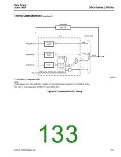
 ETC [ ETC ]