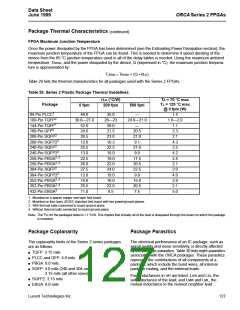
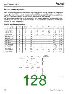
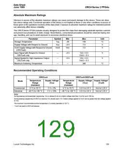
Data Sheet
June 1999
ORCA Series 2 FPGAs
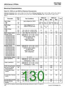
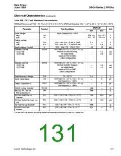
Electrical Characteristics (continued)
Table 31B. OR2TxxB Electrical Characteristics
OR2TxxB Commercial: VDD = 3.0 V to 3.6 V, 0 °C ≤ TA ≤ 70 °C; OR2TxxB Industrial: VDD = 3.0 V to 3.6 V, –40 °C ≤ TA ≤ +85°C.
OR2TxxB
Parameter
Input Voltage:
High
Low
Symbol
Test Conditions
Unit
Min
Max
Input configured as CMOS
80% VDD
GND – 0.5
VDD + 0.3
15% VDD
VIH
VIL
V
V
Output Voltage:
High
Low
VOH
VOL
VDD = min, IOH = 6 mA or 3 mA
VDD = min, IOL = 12 mA or 6 mA
2.4
—
—
0.4
V
V
IL
VDD = max, VIN = VSS or VDD
Input Leakage Current
–10
10
µA
IDDSB
OR2TxxB (TA = 25 °C, VDD = 3.3 V)
internal oscillator running,
no output loads,
Standby Current:
OR2T15B
OR2T40B
—
—
5.5
8.0
mA
mA
inputs at VDD or GND
(after configuration)
IDDSB
OR2TxxB (TA = 25 °C, VDD = 3.3 V)
internal oscillator stopped,
no output loads,
Standby Current:
OR2T15B
OR2T40B
—
—
2.0
4.5
mA
mA
inputs at VDD or GND
(after configuration)
VDR
CIN
TA = 25 °C
Data Retention Voltage
Input Capacitance
2.3
—
—
8
V
OR2TxxB (TA = 25 °C, VDD = 3.3 V)
Test frequency = 1 MHz
pF
COUT
OR2TxxB (TA = 25 °C, VDD = 3.3 V)
Test frequency = 1 MHz
Output Capacitance
—
8
pF
RDONE
RM
DONE Pull-up Resistor*
—
—
100k
100k
—
—
Ω
Ω
M3, M2, M1, and M0
Pull-up Resistors*
IPU
IPD
VDD = 3.6 V, VIN = VSS, TA = 0 °C
VDD = 3.6 V, VIN = VDD, TA = 0 °C
I/O Pad Static Pull-up
Current*
14.4
26
50.9
103
µA
µA
I/O Pad Static Pull-down Cur-
rent
RPU
RPD
VDD = all, VIN = VSS, TA = 0 °C
VDD = all, VIN = VDD, TA = 0 °C
I/O Pad Pull-up Resistor*
100k
50k
—
—
Ω
Ω
I/O Pad Pull-down
Resistor
* On the OR2TxxB devices, the pull-up resistor will externally pull the pin to a level 1.0 V below VDD.
Lucent Technologies Inc.
131

 ETC [ ETC ]