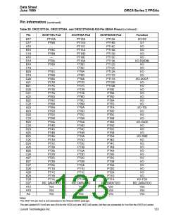
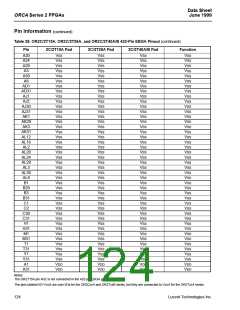
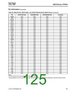
Data Sheet
June 1999
ORCA Series 2 FPGAs
Package Thermal Characteristics (continued)
FPGA Maximum Junction Temperature
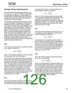
Once the power dissipated by the FPGA has been determined (see the Estimating Power Dissipation section), the
maximum junction temperature of the FPGA can be found. This is needed to determine if speed derating of the
device from the 85 °C junction temperature used in all of the delay tables is needed. Using the maximum ambient
temperature, TAmax, and the power dissipated by the device, Q (expressed in °C), the maximum junction tempera-
ture is approximated by:
TJmax = TAmax + (Q • ΘJA)
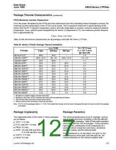
Table 29 lists the thermal characteristics for all packages used with the Series 2 FPGAs.
Table 29. Series 2 Plastic Package Thermal Guidelines
ΘJA (°C/W)
TA = 70 °C max
TJ = 125 °C max
@ 0 fpm (W)
Package
0 fpm
200 fpm
500 fpm
84-Pin PLCC1
40.0
30.0—27.0
52.0
35.0
26—23
39.0
21.5
23.0
10.3
22.5
10.0
19.0
22.0
24.0
10.0
16.0
22.0
8.5
—
24.0—21.0
—
1.4
1.8—2.0
1.1
100-Pin TQFP2
144-Pin TQFP1
160-Pin QFP2
24.0
20.5
21.0
9.1
2.3
208-Pin SQFP2
208-Pin SQFP22
240-Pin SQFP2
240-Pin SQFP22
256-Pin PBGA2, 3
256-Pin PBGA2, 4
304-Pin SQFP2
304-Pin SQFP22
352-Pin PBGA2, 3
352-Pin PBGA2, 4
432-Pin EBGA2
26.5
2.1
12.8
4.3
25.5
21.0
9.0
2.2
13.0
4.2
22.5
17.5
20.5
22.5
9.0
2.4
26.0
2.1
27.5
2.0
12.0
4.6
19.0
15.0
20.5
7.5
2.9
25.5
2.1
11.0
5.0
1. Mounted on a sparse copper one-layer test board.
2. Mounted on four-layer JEDEC standard test board with two power/ground planes.
3. With thermal balls connected to board ground plane.
4. Without thermal balls connected to board ground plane.
ψJC for the packages listed is <1 °C/W. This implies that virtually all of the heat is dissipated through the board on which the package
Note: The
is mounted.
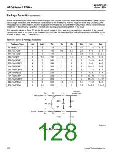
Package Coplanarity
Package Parasitics
The coplanarity limits of the Series 2 series packages
are as follows:
The electrical performance of an IC package, such as
signal quality and noise sensitivity, is directly affected
by the package parasitics. Table 30 lists eight parasitics
associated with the ORCA packages. These parasitics
represent the contributions of all components of a
package, which include the bond wires, all internal
package routing, and the external leads.
■ TQFP: 3.15 mils
■ PLCC and QFP: 4.0 mils
■ PBGA: 8.0 mils
■ SQFP: 4.0 mils (240 and 304 only)
3.15 mils (all other sizes)
Four inductances in nH are listed: LSW and LSL, the
self-inductance of the lead; and LMW and LML, the
mutual inductance to the nearest neighbor lead.
■ SQFP2: 3.15 mils
■ EBGA: 8.0 mils
Lucent Technologies Inc.
127

 ETC [ ETC ]