Data Sheet
June 1999
ORCA Series 2 FPGAs
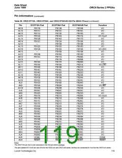
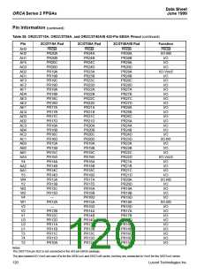
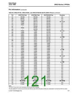
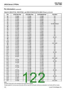
Pin Information (continued)
Table 28. OR2C/2T15A, OR2C/2T26A, and OR2C/2T40A/B 432-Pin EBGA Pinout (continued)
Pin
2C/2T15A Pad
2C/2T26A Pad
2C/2T40A/B Pad
Function
B17
C17
A18
B18
C18
A19
D18
B19
C19
B20
D19
C20
A21
B21
D20
C21
A22
B22
C22
A23
B23
D22
C23
B24
C24
D23
A25
B25
C25
D24
A26
B26
C26
A27
B27
C27
D26
A28
B28
C28
D27
A12
A16
A2
PT10A
PT9D
—
PT9C
PT9B
—
PT9A
PT8D
—
PT12A
PT11D
PT11C
PT11A
PT10D
PT10C
PT10A
PT9D
PT9C
PT9A
PT8D
PT8A
PT7D
PT7C
PT7B
PT7A
PT6D
PT6C
PT6B
PT6A
PT5D
PT5C
PT5B
PT5A
PT4D
PT4C
PT4B
PT4A
PT3D
PT3C
PT3B
PT3A
PT2D
PT2C
PT2B
PT2A
PT1D
PT1C
PT1B
PT1A
RD_DATA/TDO
VSS
PT15A
PT14D
PT14C
PT14A
PT13D
PT13C
PT13A
PT12D
PT12C
PT12A
PT11D
PT11A
PT10D
PT10A
PT9D
PT9A
PT8D
PT8A
PT7D
PT7A
PT6D
PT6C
PT6B
I/O-D2
D1
I/O
I/O
I/O
I/O
I/O-D0/DIN
I/O
I/O
I/O
I/O
PT8C
PT8B
PT8A
PT7D
PT7C
PT7B
PT7A
PT6D
PT6C
PT6B
PT6A
PT5D
PT5C
PT5B
PT5A
PT4D
PT4C
PT4B
PT4A
PT3D
PT3C
PT3B
PT3A
PT2D
PT2C
PT2B
PT2A
PT1D
PT1C
PT1B
PT1A
RD_DATA/TDO
VSS
I/O-DOUT
I/O
I/O
I/O
I/O
I/O
I/O
I/O
I/O-TDI
I/O
I/O
I/O
I/O-VDD5
I/O
I/O
I/O
I/O-TMS
I/O
PT6A
PT5D
PT5C
PT5B
PT5A
PT4D
PT4C
PT4B
I/O
I/O
I/O
I/O
I/O
I/O
I/O
I/O
PT4A
PT3D
PT3C
PT3B
PT3A
PT2D
PT2A
I/O
I/O
PT1D
PT1A
I/O-TCK
RD_DATA/TDO
VSS
RD_DATA/TDO
VSS
VSS
VSS
VSS
VSS
VSS
VSS
VSS
VSS
Notes:
The OR2T15A pin AG2 is not connected in the 432-pin EBGA package.
The pins labeled I/O-VDD5 are user I/Os for the OR2CxxA and OR2TxxB series, but they are connected to VDD5 for the OR2TxxA series.
Lucent Technologies Inc.
123

 ETC [ ETC ]