Data Sheet
June 1999
ORCA Series 2 FPGAs
Global Set/Reset (GSRN)
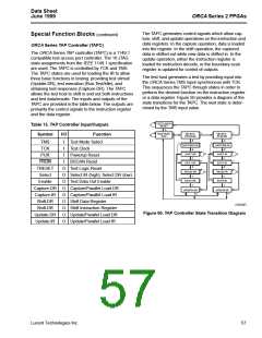
Special Function Blocks (continued)
The GSRN logic resides in the lower-right corner of the
FPGA. GSRN is an invertible, default, active-low signal
that is used to reset all of the user-accessible latches/
FFs on the device. GSRN is automatically asserted at
powerup and during configuration of the device.
Global 3-State Control (TS_ALL)
The TS_ALL block resides in the upper-right corner of
the FPGA array.
To increase the testability of the ORCA Series FPGAs,
the global 3-state function (TS_ALL) disables the
device. The TS_ALL signal is driven from either an
external pin or an internal signal. Before and during
configuration, the TS_ALL signal is driven by the input
pad RD_CFG. After configuration, the TS_ALL signal
can be disabled, driven from the RD_CFG input pad, or
driven by a general routing signal in the upper-right cor-
ner. Before configuration, TS_ALL is active-low; after
configuration, the sense of TS_ALL can be inverted.
The timing of the release of GSRN at the end of config-
uration can be programmed in the start-up logic
described below. Following configuration, GSRN may
be connected to the RESET pin via dedicated routing,
or it may be connected to any signal via normal routing.
Within each PFU, individual FFs and latches can be
programmed to either be set or reset when GSRN is
asserted.
The RESET input pad has a special relationship to
GSRN. During configuration, the RESET input pad
always initiates a configuration abort, as described in
the FPGA States of Operation section. After configura-
tion, the global set/reset signal (GSRN) can either be
disabled (the default), directly connected to the RESET
input pad, or sourced by a lower-right corner signal. If
the RESET input pad is not used as a global reset after
configuration, this pad can be used as a normal input
pad.
The following occur when TS_ALL is activated:
1. All of the user I/O output buffers are 3-stated, the
user I/O input buffers are pulled up (with the pull-
down disabled), and the input buffers are configured
with TTL input thresholds (OR2CxxA only).
2. The TDO/RD_DATA output buffer is 3-stated.
3. The RD_CFG, RESET, and PRGM input buffers remain
active with a pull-up.
4. The DONE output buffer is 3-stated, and the input
buffer is pulled-up.
Start-Up Logic
The start-up logic block is located in the lower right cor-
ner of the FPGA. This block can be configured to coor-
dinate the relative timing of the release of GSRN, the
activation of all user I/Os, and the assertion of the
DONE signal at the end of configuration. If a start-up
clock is used to time these events, the start-up clock
can come from CCLK, or it can be routed into the start-
up block using lower-right corner routing resources.
These signals are described in the Start-Up subsection
of the FPGA States of Operation section.
Internal Oscillator
The internal oscillator resides in the lower-left corner of
the FPGA array. It has output clock frequencies of
1.25 MHz and 10 MHz. The internal oscillator is the
source of the internal CCLK used for configuration. It
may also be used after configuration as a general-
purpose clock signal.
Lucent Technologies Inc.
53

 ETC [ ETC ]