Data Sheet
June 1999
ORCA Series 2 FPGAs
again. One bit of data is shifted out on RD_DATA at the
rising edge of CCLK. The first start bit of the readback
frame is transmitted out several cycles after the first ris-
ing edge of CCLK after RD_CFG is input low (see Table
48, Readback Timing Characteristics in the Timing
Characteristics section).
Special Function Blocks
Special function blocks in the Series 2 provide extra
capabilities beyond general FPGA operation. These
blocks reside in the corners of the FPGA array.
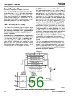
It should be noted that the RD_DATA output pin is also
used as the dedicated boundary-scan output pin, TDO.
If this pin is being used as TDO, the RD_DATA output
from readback can be routed internally to any other pin
desired. The RD_CFG input pin is also used to control
the global 3-state (TS_ALL) function. Before and during
configuration, the TS_ALL signal is always driven by
the RD_CFG input and readback is disabled. After con-
figuration, the selection as to whether this input drives
the readback or global 3-state function is determined
by a set of bit stream options. If used as the RD_CFG
input for readback, the internal TS_ALL input can be
routed internally to be driven by any input pin.
Single Function Blocks
Most of the special function blocks perform a specific
dedicated function. These functions are data/configura-
tion readback control, global 3-state control (TS_ALL),
internal oscillator generation, global set/reset (GSRN),
and start-up logic.
Readback Logic
The readback logic is located in the upper right corner
of the FPGA.
Readback is used to read back the configuration data
and, optionally, the state of the PFU outputs. A read-
back operation can be done while the FPGA is in nor-
mal system operation. The readback operation cannot
be daisy-chained. To use readback, the user selects
options in the bit stream generator in the ORCA
Foundry Development System.
The readback frame contains the configuration data
and the state of the internal logic. During readback, the
value of all five PFU outputs can be captured. The fol-
lowing options are allowed when doing a capture of the
PFU outputs.
1. Do not capture data (the data written to the capture
RAMs, usually 0, will be read back).
Table 11 provides readback options selected in the bit
stream generator tool. The table provides the number
of times that the configuration data can be read back.
This is intended primarily to give the user control over
the security of the FPGA’s configuration program. The
user can prohibit readback (0), allow a single readback
(1), or allow unrestricted readback (U).
2. Capture data upon entering readback.
3. Capture data based upon a configurable signal
internal to the FPGA. If this signal is tied to
logic 0, capture RAMs are written continuously.
4. Capture data on either options 2 or 3 above.
The readback frame has a similar, but not identical, for-
mat to the configuration frame. This eases a bitwise
comparison between the configuration and readback
data. The readback data is not inverted. Every data
frame has one low start bit and one high stop bit. The
preamble, including the length count field, is not part of
the readback frame. The readback frame contains
states in locations not used in the configuration. These
locations need to be masked out when comparing the
configuration and readback frames. The development
system optionally provides a readback bit stream to
compare to readback from the FPGA. Also note that if
any of the LUTs are used as RAM and new data is writ-
ten to them, these bits will not have the same values as
the original configuration data frame either.
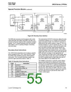
Table 11. Readback Options
Option
Function
Prohibit Readback
0
1
Allow One Readback Only
U
Allow Unrestricted Number of Readbacks
The pins used for readback are readback data
(RD_DATA), read configuration (RD_CFG), and configu-
ration clock (CCLK). A readback operation is initiated
by a high-to-low transition on RD_CFG. The RD_CFG
input must remain low during the readback operation.
The readback operation can be restarted at frame 0 by
driving the RD_CFG pin high, applying at least two ris-
ing edges of CCLK, and then driving RD_CFG low
52
Lucent Technologies Inc.

 ETC [ ETC ]