Data Sheet
June 1999
ORCA Series 2 FPGAs
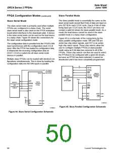
Synchronous Peripheral Mode
FPGA Configuration Modes (continued)
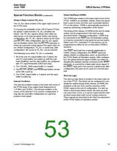
In the synchronous peripheral mode, byte-wide data is
input into D[7:0] on the rising edge of the CCLK input.
The first data byte is clocked in on the second CCLK
after INIT goes high. Subsequent data bytes are
clocked in on every eighth rising edge of CCLK. The
RDY signal is an output which acts as an acknowledge.
RDY goes high one CCLK after data is clocked and,
after one CCLK cycle, returns low. The process repeats
until all of the data is loaded into the FPGA. The data
begins shifting on DOUT 1.5 cycles after it is loaded in
parallel. It requires additional CCLKs after the last byte
is loaded to complete the shifting. Figure 43 shows the
connections for synchronous peripheral mode.
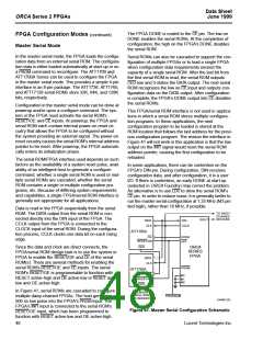
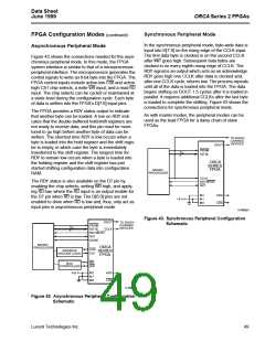
Asynchronous Peripheral Mode
Figure 42 shows the connections needed for the asyn-
chronous peripheral mode. In this mode, the FPGA
system interface is similar to that of a microprocessor-
peripheral interface. The microprocessor generates the
control signals to write an 8-bit byte into the FPGA. The
FPGA control inputs include active-low CS0 and active-
high CS1 chip selects, a write WR input, and a read RD
input. The chip selects can be cycled or maintained at
a static level during the configuration cycle. Each byte
of data is written into the FPGA’s D[7:0] input pins.
The FPGA provides a RDY status output to indicate
that another byte can be loaded. A low on RDY indi-
cates that the double-buffered hold/shift registers are
not ready to receive data, and this pin must be moni-
tored to go high before another byte of data can be
written. The shortest time RDY is low occurs when a
byte is loaded into the hold register and the shift regis-
ter is empty, in which case the byte is immediately
transferred to the shift register. The longest time for
RDY to remain low occurs when a byte is loaded into
the holding register and the shift register has just
started shifting configuration data into configuration
RAM.
As with master modes, the peripheral modes can be
used as the lead FPGA for a daisy chain of slave
FPGAs.
TO DAISY-
CHAINED
DEVICES
DOUT
PRGM
D[7:0]
8
ORCA
SERIES
FPGA
MICRO-
PROCESSOR
CCLK
The RDY status is also available on the D7 pin by
enabling the chip selects, setting WR high, and apply-
ing RD low, where the RD input is an output enable for
the D7 pin when RD is low. The D[6:0] pins are not
enabled to drive when RD is low and, thus, only act as
input pins in asynchronous peripheral mode.
RDY/BUSY
INIT
M2
M1
M0
HDC
LDC
+5 V
5-4486(F)
Figure 43. Synchronous Peripheral Configuration
Schematic
DOUT
CCLK
TO DAISY-
CHAINED
DEVICES
PRGM
D[7:0]
8
RDY/BUSY
INIT
DONE
MICRO-
PROCESSOR
ORCA
SERIES
FPGA
CS0
CS1
ADDRESS
DECODE LOGIC
RD
WR
BUS
CONTROLLER
VDD
M2
M1
M0
HDC
LDC
5-4484(F)
Figure 42. Asynchronous Peripheral Configuration
Schematic
Lucent Technologies Inc.
49

 ETC [ ETC ]