Data Sheet
June 1999
ORCA Series 2 FPGAs
Special Function Blocks (continued)
CCLK
CCLK
DIN
CCLK
DOUT
DIN
DOUT
A[17:0]
DOUT
A[17:0]
EPROM
ORCA
SERIES
FPGA
ORCA
SERIES
FPGA
ORCA
SERIES
FPGA
D[7:0]
D[7:0]
DONE
MASTER
SLAVE #1
SLAVE #2
VDD
OE
CE
DONE
PRGM
DONE
PRGM
PRGM
VDD
INIT
INIT
VDD
INIT
PROGRAM
VDD
M2
M1
M0
HDC
LDC
RCLK
HDC
LDC
RCLK
VDD
M2
M1
M0
M2
M1
M0
HDC
LDC
VDD OR
GND
RCLK
5-4488(F)
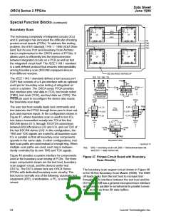
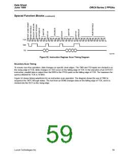
Figure 48. Boundary-Scan Interface
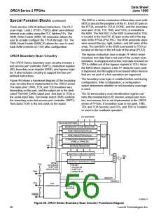
The BSM also increases test throughput with a dedi-
cated automatic test-pattern generator and with com-
pression of the test response with a signature analysis
register. The PC-based boundary-scan test card/soft-
ware allows a user to quickly prototype a boundary-
scan test setup.
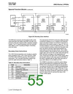
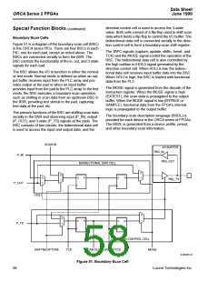
The external test (EXTEST) instruction allows the inter-
connections between ICs in a system to be tested for
opens and stuck-at faults. If an EXTEST instruction is
performed for the system shown in Figure 47, the con-
nections between U1 and U2 (shown by nets a, b, and
c) can be tested by driving a value onto the given nets
from one device and then determining whether the
same value is seen at the other device. This is deter-
mined by shifting 2 bits of data for each pin (one for the
output value and one for the 3-state value) through the
BSR until each one aligns to the appropriate pin.
Then, based upon the value of the 3-state signal, either
the I/O pad is driven to the value given in the BSR, or
the BSR is updated with the input value from the I/O
pad, which allows it to be shifted out TDO.
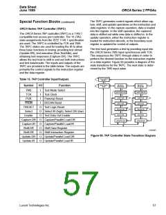
Boundary-Scan Instructions
The ORCA Series boundary-scan circuitry is used for
three mandatory IEEE 1149.1 tests (EXTEST, SAM-
PLE/PRELOAD, BYPASS) and four ORCA-defined
instructions. The 3-bit wide instruction register sup-
ports the eight instructions listed in Table 12.
The SAMPLE instruction is useful for system debug-
ging and fault diagnosis by allowing the data at the
FPGA’s I/Os to be observed during normal operation.
The data for all of the I/Os is captured simultaneously
into the BSR, allowing them to be shifted-out TDO to
the test host. Since each I/O buffer in the PICs is bidi-
rectional, two pieces of data are captured for each I/O
pad: the value at the I/O pad and the value of the
3-state control signal.
Table 12. Boundary-Scan Instructions
Code
000
001
010
011
100
101
110
111
Instruction
EXTEST
PLC Scan Ring 1
RAM Write (RAM_W)
Reserved
SAMPLE/PRELOAD
PLC Scan Ring 2
RAM Read (RAM_R)
BYPASS
Lucent Technologies Inc.
55

 ETC [ ETC ]