Data Sheet
June 1999
ORCA Series 2 FPGAs
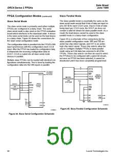
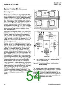
on the negative edge of CCLK. Figure 46 shows the
connections for loading multiple FPGAs in a daisy-
chain configuration.
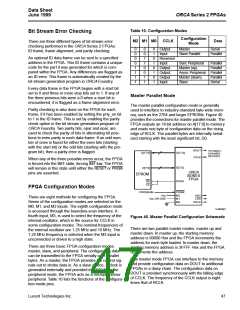
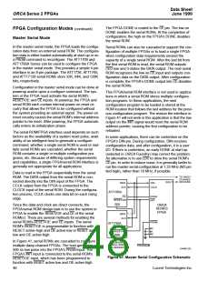
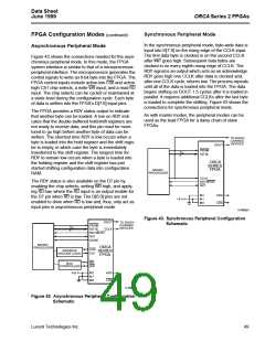
FPGA Configuration Modes (continued)
Daisy Chain
The generation of CCLK for the daisy-chained devices
which are in slave serial mode differs depending on the
configuration mode of the lead device. A master paral-
lel mode device uses its internal timing generator to
produce an internal CCLK at eight times its memory
address rate (RCLK). The asynchronous peripheral
mode device outputs eight CCLKs for each write cycle.
If the lead device is configured in either synchronous
peripheral or a slave mode, CCLK is routed to the lead
device and to all of the daisy-chained devices.
Multiple FPGAs can be configured by using a daisy
chain of the FPGAs. Daisy chaining uses a lead FPGA
and one or more FPGAs configured in slave serial
mode. The lead FPGA can be configured in any mode
except slave parallel mode. (Daisy chaining is not avail-
able with the boundary-scan ram_w instruction, dis-
cussed later.)
All daisy-chained FPGAs are connected in series.
Each FPGA reads and shifts the preamble and length
count in on positive CCLK and out on negative CCLK
edges.
The development system can create a composite
configuration bit stream for configuring daisy-chained
FPGAs. The frame format is a preamble, a length count
for the total bit stream, multiple concatenated data
frames, an end-of-configuration frame per device, a
postamble, and an additional fill bit per device in the
serial chain.
An upstream FPGA that has received the preamble
and length count outputs a high on DOUT until it has
received the appropriate number of data frames so that
downstream FPGAs do not receive frame start bits
(0s). After loading and retransmitting the preamble and
length count to a daisy chain of slave devices, the lead
device loads its configuration data frames. The loading
of configuration data continues after the lead device
has received its configuration data if its internal frame
bit counter has not reached the length count. When the
configuration RAM is full and the number of bits
received is less than the length count field, the FPGA
shifts any additional data out on DOUT.
As seen in Figure 46, the INIT pins for all of the FPGAs
are connected together. This is required to guarantee
that powerup and initialization will work correctly. In
general, the DONE pins for all of the FPGAs are also
connected together as shown to guarantee that all of
the FPGAs enter the start-up state simultaneously. This
may not be required, depending upon the start-up
sequence desired.
The configuration data is read into DIN of slave devices
on the positive edge of CCLK, and shifted out DOUT
CCLK
CCLK
CCLK
DIN
DOUT
DIN
DOUT
A[17:0]
DOUT
A[17:0]
EPROM
ORCA
SERIES
FPGA
ORCA
SERIES
FPGA
ORCA
SERIES
FPGA
D[7:0]
D[7:0]
DONE
MASTER
SLAVE #1
SLAVE #2
VDD
OE
CE
DONE
PRGM
DONE
PRGM
PRGM
VDD
INIT
INIT
VDD
INIT
PROGRAM
VDD
M2
M1
M0
HDC
LDC
RCLK
HDC
LDC
RCLK
VDD
M2
M1
M0
M2
M1
M0
HDC
VDD OR
LDC
RCLK
GND
5-4488(F)
Figure 46. Daisy-Chain Configuration Schematic
Lucent Technologies Inc.
51

 ETC [ ETC ]