Data Sheet
June 1999
ORCA Series 2 FPGAs
The write address (WA[3:0]) and write data (WD[3:0])
are also latched by the RAM clock in order to simplify
the timing. Reading data from the RAM is done asyn-
chronously; thus, the read address (RA[3:0]) is not
latched. The result from the read operation is placed on
the LUT outputs (F[3:0]). The F[3:0] data outputs can
be routed out of the PFU or sent to the latch/FF D[3:0]
inputs.
Programmable Logic Cells (continued)
Synchronous Memory Modes—SSPM and SDPM
The MA/MB asynchronous memory modes described
previously allow the PFU to perform as a 16 x 4
(64 bits) single-port RAM. Synchronously writing to this
RAM requires the write-enable control signal to be
gated with the clock in another PFU to create a write
pulse. To simplify this functionality, the Series 2 devices
contain a synchronous single-port memory (SSPM)
mode, where the generation of the write pulse is done
in each PFU.
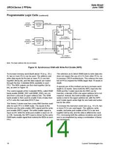
There are two ways to use the latches/FFs in conjunc-
tion with the SSPM. If the phase of the latch/FF clock
and the RAM clock are the same, only a read address
or write address can be supplied to the RAM that
meets the synchronous timing requirements of both
the RAM clock and latch/FF clock. Therefore, either a
write to the RAM or a read from the RAM can be done
in each clock cycle, but not both. If the RAM clock is
inverted from the latch/FF clock, then both a write to
the RAM and a read from the RAM can occur in each
clock cycle. This is done by adding an external write
address/read address multiplexer as shown in
Figure 15.
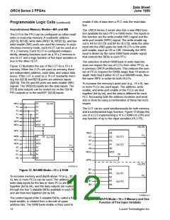
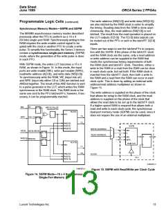
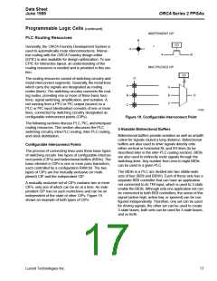
With SSPM mode, the entire LUT becomes a 16 x 4
RAM, as shown in Figure 14. In this mode, the input
ports are write enable (WE), write-port enable (WPE),
read/write address (A[3:0]), and write data (WD[3:0]).
To synchronously write the RAM, WE (input into a4)
and WPE (input into either C0 or CIN) are latched and
ANDed together. The result of this AND function is sent
to a pulse generator in the LUT, which writes the RAM
synchronous to the RAM clock. This RAM clock is the
same one sent to the PFU latches/FFs; however, if nec-
essary, it can be programmably inverted.
The write address is supplied on the phase of the clock
that allows for setup to the RAM clock, and the read
address is supplied on the phase of the clock that
allows the read data to be set up to the latch/FF clock.
If a higher-speed RAM is required that allows both a
read and write in each clock cycle, the synchronous
dual-port memory mode (SDPM) can be used, since it
does not require the use of an external multiplexer.
A4
WE
WRITE PULSE
GENERATOR
D
D
Q
Q
HLUTA
WR
F3
F2
WPE
CIN, C0
WA[3:0]
RA[3:0]
SSPM
WD[3:2]
WRITE ADDRESS
1
0
WD
A
A[3:0]
A[3:0], B[3:0]
WD[3:0]
D
D
Q
READ ADDRESS
D
Q
WE
WD[3:0]
WPE
Q
HLUTB
RAM CLK
WR
F1
F0
WA[3:0]
RA[3:0]
WD[1:0]
CLOCK
PFU
5-4644(F).r1
5-4642(F).r1
Figure 15. SSPM with Read/Write per Clock Cycle
Figure 14. SSPM Mode—16 x 4 Synchronous
Single-Port Memory
Lucent Technologies Inc.
13

 ETC [ ETC ]