Data Sheet
June 1999
ORCA Series 2 FPGAs
enable 4 bits of data from a PLC onto the read data
bus.
Programmable Logic Cells (continued)
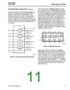
Asynchronous Memory Modes—MA and MB
The ORCA Series 2 series also has a new AND func-
tion available for each PFU in RAM mode. The inputs to
this function are the write-enable (WE) signal and the
write-port enable (WPE) signal. The write-enable sig-
nal is A4 for HLUTA and B4 for HLUTB, while the other
input into the AND gates for both HLUTs is the write-
port enable, input on C0 or CIN. Generally, the WPE
input is driven by the same RAM bank-enable signal
that controls the BIDIs in each PFU.
The LUT in the PFU can be configured as either read/
write or read-only memory. A read/write address
(A[3:0], B[3:0]), write data (WD[1:0], WD[3:2]), and two
write-enable (WE) ports are used for memory. In asyn-
chronous memory mode, each HLUT can be used as a
16 x 2 memory. Each HLUT is configured indepen-
dently, allowing functions such as a 16 x 2 memory in
one HLUT and a logic function of five input variables or
less in the other HLUT.
The selection of which RAM bank to write data into
does not require the use of LUTs from other PFUs, as
in previous ORCA architectures. This reduces the num-
ber of PFUs required for RAMs larger than 16 words in
depth. Note that if either HLUT is in MA/MB mode, then
the same WPE is active for both HLUTs.
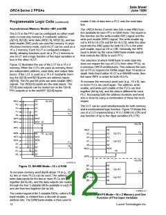
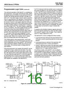
Figure 12 illustrates the use of the LUT for a 16 x 4
memory. When the LUTs are used as memory, there
are independent address, input data, and output data
buses. If the LUT is used as a 16 x 4 read/write mem-
ory, the A[3:0] and B[3:0] ports are address inputs
(A[3:0]). The A4 and B4 ports are write-enable (WE)
signals. The WD[3:0] inputs are the data inputs. The
F[3:0] data outputs can be routed out on the O[4:0]
PFU outputs or to the latch/FF D[3:0] inputs.
To increase the memory’s word size (e.g., 16 x 8), two
or more PLCs are used again. The address, write-
enable, and write-port enable of the PLCs are tied
together (bit by bit), and the data is different for each
PLC. Increasing both the address locations and word
size is done by using a combination of these two tech-
niques.
WEA
A3
A4
HLUTA
A3
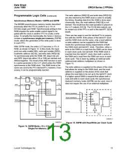
The LUT can be used simultaneously for both memory
and a combinatorial logic function. Figure 13 shows the
use of a LUT implementing a 16 x 2 RAM (HLUTA) and
any function of up to five input variables (HLUTB).
A2
A2
F3
F2
A1
A1
A0
A0
WD3
WD2
WD3
WD2 C0
HLUTA
WPE
WEA
A3
A4
F3
F2
WEB
WD1
WD0
B3
QLUT3
QLUT2
B4
C0
HLUTB
A3
WD1
WD0
B3
A2
A2
A1
A1
F1
F0
A0
A0
B2
B2
WD3
WD3
C0
B1
B1
B0
B0
WPE
HLUTB
F0
5-2757(F).r3
B4
B3
B2
B1
B0
B4
B3
B2
B1
B0
Figure 12. MA/MB Mode—16 x 4 RAM
QLUT1
QLUT0
To increase memory word depth above 16 (e.g., 32 x
4), two or more PLCs can be used. The address and
write data inputs for the two or more PLCs are tied
together (bit by bit), and the data outputs are routed
through the four 3-statable BIDIs available in each PFU
and are then tied together (bit by bit).
5-2845(F).a.r1
The control signal of the 3-statable BIDIs, called a RAM
bank-enable, is created from a decode of upper
address bits. The RAM bank-enable is then used to
Figure 13. MA/F5 Mode—16 x 2 Memory and One
Function of Five Input Variables
12
Lucent Technologies Inc.

 ETC [ ETC ]