Data Sheet
June 1999
ORCA Series 2 FPGAs
Latches/Flip-Flops
Programmable Logic Cells (continued)
The four latches/FFs in the PFU can be used in a vari-
ety of configurations. In some cases, the configuration
options apply to all four latches/FFs in the PFU. For
other options, each latch/FF is independently program-
mable.
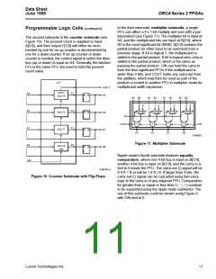
A4
WE
WRITE PULSE
GENERATOR
D
D
Q
Q
HLUTA
WR
F3
F2
WPE
CIN, C0
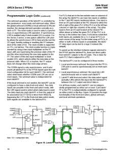
Table 4 summarizes these latch/FF options. The
WA[3:0]
RA[3:0]
latches/FFs can be configured as either positive or
negative level-sensitive latches, or positive or negative
edge-triggered flip-flops. All latches/FFs in a given PFU
share the same clock, and the clock to these latches/
FFs can be inverted. The input into each latch/FF is
from either the corresponding QLUT output (F[3:0]) or
the direct data input (WD[3:0]). For latches/FFs located
in the two outer rings of PLCs, additional inputs are
possible. These additional inputs are fast paths from
I/O pads located in PICs in the same row or column as
the PLCs. If the latch/FF is not located in the two outer
rings of the PLCs, the latch/FF input can also be tied to
logic 0, which is the default. The four latch/FF outputs,
Q[3:0], can be placed on the five PFU outputs, O[4:0].
WD[1:0]
WA[3:0]
WD[1:0]
A[3:0]
D
D
Q
WD[1:0]
Q
HLUTB
WR
F1
F0
WA[3:0]
RA[3:0]
WD[1:0]
RA[3:0]
B[3:0]
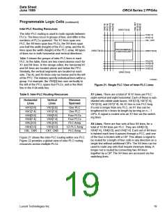
5-4641(F).r1
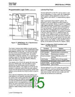
Figure 17. SDPM Mode—16 x 2 Synchronous
Dual-Port Memory
Table 4. Configuration RAM Controlled Latch/
Flip-Flop Operation
The Series 2 devices have added a second synchro-
nous memory mode known as the synchronous dual-
port memory (SDPM) mode. This mode writes data
into the memory synchronously in the same manner
described previously for SSPM mode. The SDPM
mode differs in that two separate 16 x 2 memories are
created in each PFU that have the same WE, WPE,
write data (WD[1:0]), and write address (WA[3:0])
inputs, as shown in Figure 17.
Function
Options
Functionality Common to All Latch/FFs in PFU
LSR Operation
Clock Polarity
Asynchronous or synchronous
Noninverted or inverted
Front-End Select Direct (WD[3:0]) or from LUT
(F[3:0])
LSR Priority
Either LSR or CE has priority
Functionality Set Individually in Each Latch/FF in PFU
The outputs of HLUTA (F[3:2]) operate the same way
they do in SSPM mode—the read address comes
directly from the A[3:0] inputs used to create the
latched write address. The outputs of HLUTB (F[1:0])
operate in a dual-port mode where the write address
comes from the latched version of A[3:0], and the read
address comes directly from RA[3:0], which is input on
B[3:0].
Latch/FF Mode
Set/Reset Mode
Latch or flip-flop
Set or Reset
The four latches/FFs in a PFU share the clock (CK),
clock enable (CE), and local set/reset (LSR) inputs.
When CE is disabled, each latch/FF retains its previous
value when clocked. Both the clock enable and LSR
inputs can be inverted to be active-low.
Since external multiplexing of the write address and
read address is not required, extremely fast RAMs can
be created. New system applications that require an
interface between two different asynchronous clocks
can also be implemented using the SDPM mode. An
example of this is accomplished by creating FIFOs
where one clock controls the synchronous write of data
into the FIFO, and the other clock controls the read
address to allow reading of data at any time from the
FIFO.
Lucent Technologies Inc.
15

 ETC [ ETC ]