Data Sheet
June 1999
ORCA Series 2 FPGAs
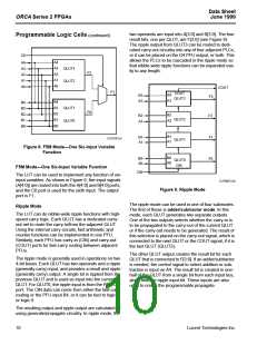
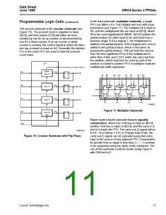
Programmable Logic Cells (continued)
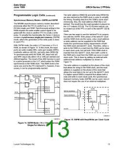
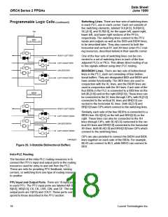
UPPER
ADDRESS
BITS
ADDRESS
DECODE
LUT1
BANK_EN1
WPE
4
DI
DO
WR
BIDI
16 x 4 RAM +
4 BUFFERS/PFU
4
DOUT
UPPER
ADDRESS
BITS
ADDRESS
DECODE
LUT2
BANK_EN2
WPE
4
4
DIN
WR
DI
DO
WR
BIDI
CLK
16 x 4 RAM +
4 BUFFERS/PFU
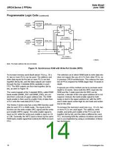
5-4640(F)
Note: The lower address bits are not shown.
Figure 16. Synchronous RAM with Write-Port Enable (WPE)
To increase memory word depth above 16 (e.g., 32 x
4), two or more PLCs can be used. The address and
write data inputs for the two or more PLCs are tied
together (bit by bit), and the data outputs are routed
through the four 3-statable BIDIs available in each
PFU. The BIDI outputs are then tied together (bit by
bit), as seen in Figure 16.
The selection as to which RAM bank to write data into
does not require the use of LUTs from other PFUs, as
in previous ORCA architectures. This reduces the num-
ber of PFUs required for RAMs larger than 16 words in
depth.
A special use of this method can be to increase word
depth to 32 words. Since both the WPE input into the
RAM and the 3-state input into the BIDI can be
inverted, a decode of the one upper address bit is not
required. Instead, the bank-enable signal for both
banks is tied to the upper address bit, with the WPE
and 3-state inputs active-high for one bank and active-
low for the other.
The control signals of the 3-statable BIDIs, called RAM
bank-enable (BANK_EN1 and BANK_EN2), are cre-
ated from a decode of upper address bits. The RAM
bank-enable is then used to enable 4 bits of data from
a PLC onto the read data (DOUT) bus.
The Series 2 series now has a new AND function avail-
able for each PFU in RAM mode. The inputs to this
function are the write-enable (WE) signal and the write-
port enable (WPE) signal. The write-enable signal is
input on A4, while the write-port enable is input on C0
or CIN. Generally, the WPE input is driven by the same
RAM bank-enable signal that controls the BIDIs in each
PFU.
To increase the memory’s word size (e.g., 16 x 8), two
or more PLCs are used again. The address, write-
enable, and write-port enable of the PLCs are tied
together (bit by bit), and the data is different for each
PLC. Increasing both the address locations and word
size is accomplished by using a combination of these
two techniques.
14
Lucent Technologies Inc.

 ETC [ ETC ]