Data Sheet
June 1999
ORCA Series 2 FPGAs
Timing Characteristics (continued)
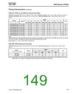
Table 42A. OR2CxxA and OR2TxxA Internal Clock Delay
OR2CxxA Commercial: VDD = 5.0 V ± 5%, 0 °C ≤ TA ≤ 70 °C; OR2CxxA Industrial: VDD = 5.0 V ± 10%, –40 °C ≤ TA ≤ +85 °C.
OR2TxxA Commercial: VDD = 3.0 V to 3.6 V, 0 °C ≤ TA ≤ 70 °C; OR2TxxA Industrial: VDD = 3.0 V to 3.6 V, –40 °C ≤ TA ≤
+85 °C.
Speed
Device
(TJ = 85 °C, VDD = min)
Symbol
-2
-3
-4
-5
-6
-7
Unit
Min
—
—
—
—
—
—
—
—
Max
4.6
4.7
4.8
4.9
5.0
5.1
5.2
5.6
Min
—
—
—
—
—
—
—
—
Max
4.4
4.5
4.6
4.7
4.8
4.9
5.1
5.4
Min
—
—
—
—
—
—
—
—
Max
4.3
4.4
4.5
4.6
4.7
4.8
5.0
5.3
Min
—
—
—
—
—
—
—
—
Max
3.6
3.7
3.8
3.9
4.0
4.1
4.2
4.5
Min
—
—
—
—
—
—
—
—
Max
—
Min
—
—
—
—
—
—
—
—
Max
—
OR2C04A/OR2T04A
OR2C06A/OR2T06A
OR2C08A/OR2T08A
OR2C10A/OR2T10A
OR2C12A/OR2T12A
OR2C15A/OR2T15A
OR2C26A/OR2T26A
OR2C40A/OR2T40A
CLK_DEL
CLK_DEL
CLK_DEL
CLK_DEL
CLK_DEL
CLK_DEL
CLK_DEL
CLK_DEL
ns
ns
ns
ns
ns
ns
ns
ns
—
—
—
—
—
—
—
—
3.9
4.0
4.2
3.3
3.4
3.6
Notes:
This clock delay is for a fully routed clock tree that uses the primary clock network. It includes both the input buffer delay and the clock routing
to the PFU CLK input. The delay will be reduced if any of the clock branches are not used.
Speed grades of -5, -6, and -7 are for OR2TxxA devices only.
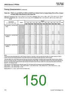
Table 42B. OR2TxxB Internal Clock Delay
OR2TxxB Commercial: VDD = 3.0 V to 3.6 V, 0 °C ≤ TA ≤ 70 °C; OR2TxxB Industrial: VDD = 3.0 V to 3.6 V, –40 °C ≤ TA ≤
+85 °C.
Speed
Device
(TJ = 85 °C, VDD = min)
Symbol
-7
-8
Unit
Min
—
Max
3.6
Min
—
Max
3.1
OR2T15B
OR2T40B
CLK_DEL
CLK_DEL
ns
ns
—
3.8
—
3.3
Note: This clock delay is for a fully routed clock tree that uses the primary clock network. It includes both the input buffer delay and the clock
routing to the PFU CLK input. The delay will be reduced if any of the clock branches are not used.
Lucent Technologies Inc.
149

 ETC [ ETC ]