MITSUBISHI MICROCOMPUTERS
7470/7471 Group
SINGLE-CHIP 8-BIT CMOS MICROCOMPUTER
A-D CONVERTER
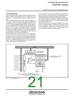
The A-D conversion register (address 00DA16) contains informa-
tion on the results of conversion, so that it is possible to know the
results of conversion by reading the contents of this register.
The following explains the procedure to execute A-D conversion.
First, set values to bit 2 to bit 0 in the A-D control register to select
the pins that you want to execute A-D conversion. Next, clear the
A-D conversion end bit to “0”.
The A-D conversion uses an 8-bit successive comparison method.
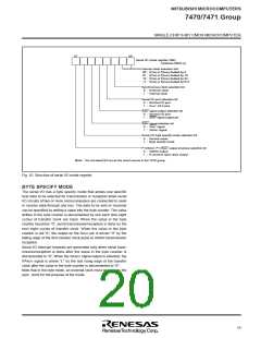
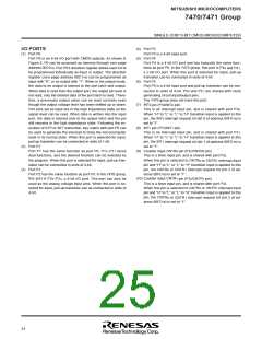
Figure 11 shows a block diagram of the A-D conversion circuit.
Conversion is automatically carried out once started by the pro-
gram.
There are eight analog input pins which are shared with P20 to
P27 of port P2 (Only P20 to P23 4-bit for 7470 group. Which ana-
log inputs are to be A-D converted is specified by using bit 2 to bit
0 in the A-D control register (address 00D916). Pins for inputs to
be A-D converted must be set for input by setting the direction reg-
ister bit to “0”. Bit 3 in the A-D control register is an A-D conversion
end bit. This is “0” during A-D conversion; it is set to “1” when the
conversion is terminated. Therefore, it is possible to know whether
A-D conversion is terminated by checking this bit. Bit 4 in the A-D
control register is a VREF connection selection bit.
When the above is done, A-D conversion is initiated. The A-D con-
version is completed after an elapse of 50 machine cycles
(12.5 µs when f(XIN)= 8 MHz), the A-D conversion end bit is set to
“1”, and the interrupt request bit is set to “1”. The results of conver-
sion are contained in the A-D conversion register.
During A-D conversion, this bit must be set “1” for the ladder resis-
tor and VREF pin to be connected; after the A-D conversion is
terminated, this bit can be reset to “0” to separate the ladder resis-
tor from the VREF pin. In this way, power consumption in the ladder
resistor can be suppressed while no A-D conversion is performed.
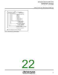
Figure 13 shows the relationship between the contents of A-D
control register and the selected input pins.
Data bus
bit 4
bit 0
A-D control register
(Address 00D916
)
P20/IN0
A-D conversion completion
interrupt request
A-D control circuit
P21
P22
P23
P24
P25
P26
P27
/IN1
/IN2
/IN3
/IN4
/IN5
/IN6
/IN7
A-D conversion register
Comparator
(Address 00DA16
)
Switch tree
Ladder resistor
V
SS (Note 1)
V
REF
Notes 1 : AVSS for M37471M2/M4/M8/E4/E8-XXXFP
2 : 7470 group does not have P2 /IN to P2 /IN7 pins.
4
4
7
Fig. 11 A-D converter circuit
20

 ETC [ ETC ]