MITSUBISHI MICROCOMPUTERS
7470/7471 Group
SINGLE-CHIP 8-BIT CMOS MICROCOMPUTER
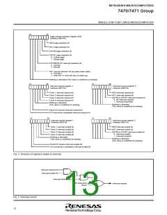
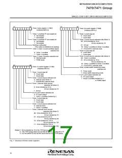
b7
b0
b7
b0
Timer mode register 2 (TM2)
(Address 00FA16
Timer 34 mode register (T34M)
)
(Address 00F916
)
Timer 3 count stop bit
0 : Count start
Timer 1 overflow FF set enable bit
0 : Set disable
1 : Count stop
1 : Set enable
Timer 4 overflow FF set enable bit
0 : Set disable
Timer 3 count source selection bits (Note 3)
00 : f(XIN) divided by 16 or
1 : Set enable
f(XCIN) divided by 16
01 : f(XCIN
10 : Timer 1 overflow or timer 2 overflow
11 : P3 /CNTR external clock
)
Nothing is allocated
(The value is undefined at reading)
Timer 3, timer 4 count overflow signal
selection bit
3
1
Timer 4 count stop bit
0 : Count start
0 : Timer 1 overflow
1 : Timer 2 overflow
1 : Count stop
Timer 4 count source selection bits (Note 3)
00 : Timer 3 overflow
Timer 3, timer 4 function selection bit
0 : Normal mode
01 : f(XIN) divided by 16 or
f(XCIN) divided by 16
1 : PWM mode
10 : Timer 1 overflow or timer 2 overflow
11 : P33/CNTR1 external clock
Timer 4 pulse width measuring mode
selection bit
b7
b0
Timer 12 mode register (T12M)
(Address 00F816
)
0 : Timer mode
1 : Pulse width measuring mode
Timer 1 count stop bit
0 : Count start
1 : Count stop
Timer 1 count source selection bit
0 : Internal clock (Note 1)
P1
0 : P1
3
/T
1
port output selection bit
port output
3
1 : Timer 4 overflow divided by 2
or PWM output
1 : P3
Timer 1 internal clock source
selection bit (Note 2)
0 : f(XIN) divided by 16 or
f(XCIN) divided by 16
2/CNTR0 external clock
1 : f(XCIN
P1 /T port output selection bit
0 : P1 port output
)
2
0
2
1 : Timer 1 overflow divided by 2
Timer 2 count stop bit
0 : Count start
1 : Count stop
Timer 2 count source selection bit
0 : Internal clock
1 : Timer 1 overflow
Timer 2 internal clock source
selection bits (Note 3)
00 : f(XIN) divided by 16 or
f(XCIN) divided by 16
01 : f(XIN) divided by 64 or
f(XCIN) divided by 64
10 : f(XIN) divided by 128 or
f(XCIN) divided by 128
11 : f(XIN) divided by 256 or
f(XCIN) divided by 256
Notes 1 : f(XIN) divided by 16 in the 7470 group.
2 : The 7470 group does not use this bit (bit 2). Set this bit to “0”.
3 : Do not select f(XCIN) as the count source in the 7470 group.
Fig. 7 Structure of timer mode registers
16

 ETC [ ETC ]