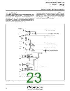
MITSUBISHI MICROCOMPUTERS
7470/7471 Group
SINGLE-CHIP 8-BIT CMOS MICROCOMPUTER
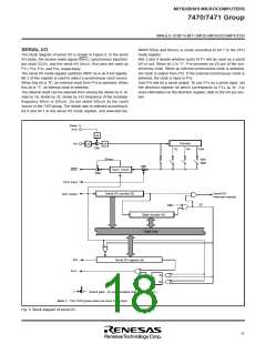
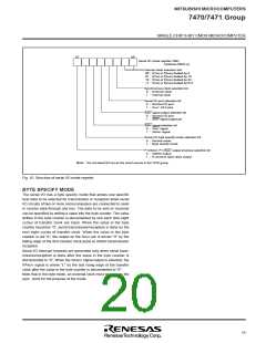
Bit 4 determines if P17 is used as an output pin for the receive
ready signal (bit 4=“1”, SRDY) or used as a normal I/O pin (bit
4=“0”).
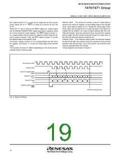
Internal Clock – The serial I/O counter is set to 7 when data is
stored in the serial I/O register. At each falling edge of the transfer
clock, serial data is output to P15. During the rising edge of this
clock, data can be input from P14 and the data in the serial I/O
register will be shifted 1 bit. Data is output starting with the LSB.
After the transfer clock has counted 8 times, the serial I/O register
will be empty and the transfer clock will remain at a high level. At
this time the interrupt request bit will be set.
When the P17 pin is used as the SRDY output pin, output signal
can be selected between SRDY signal and SARDY signal by using
bit 5 in the serial I/O mode register. The SRDY signal is driven “L”
by a signal written into the serial I/O register to inform that the de-
vice is ready to receive. Then, the SRDY signal is driven “H” on the
first falling edge of the transfer clock.
External Clock – If an external clock is used, the interrupt request
bit will be set after the transfer clock has counted 8 times but the
transfer clock will not stop. Due to this reason, the external clock
must be controlled from the outside.
The SARDY signal is driven “H” by a signal written into the serial
I/O register, and driven “L” on the last rising edge of the transfer
clock.
The function of serial I/O differs depending on the clock source;
external clock or internal clock.
Timing diagrams are shown in Figure 9.
Synchronous clock
Transfer clock
Serial I/O register write
signal
Serial I/O output
D0
D1
D2
D3
D4
D5
D6
D7
SOUT
Serial I/O input
SIN
Receive ready signal
SRDY
Interrupt request bit set
Fig. 9 Serial I/O timing
18

 ETC [ ETC ]