MITSUBISHI MICROCOMPUTERS
7470/7471 Group
SINGLE-CHIP 8-BIT CMOS MICROCOMPUTER
SERIAL I/O
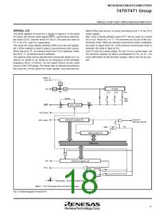
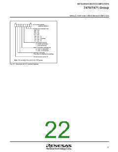
tween f(XIN) and f(XCIN) is mode according to bit 7 in the CPU
mode register.
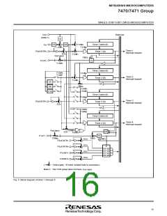
The block diagram of serial I/O is shown in Figure 8. In the serial
I/O mode, the receive ready signal (SRDY), synchronous input/out-
put clock (CLK), and the serial I/O (SOUT, SIN) pins are used as
P17, P16, P15, and P14, respectively.
Bits 3 and 4 decide whether parts of P1 will be used as a serial
I/O or not. When bit 3 is “1”, P16 becomes an I/O pin of the syn-
chronous clock. When an internal synchronous clock is selected,
the clock is output from P16. If the external synchronous clock is
selected, the clock is input to P16.
The serial I/O mode register (address 00DC16) is an 8-bit register.
Bit 2 of this register is used to select a synchronous clock source.
When this bit is “0”, an external clock from P16 is selected. When
this bit is “1”, an internal clock is selected.
And P15 will be a serial output. To use P14 as a serial input, set
the direction register bit which corresponds to P14, to “0”. For
more information on the direction register, refer to the I/O pin sec-
tion.
The internal clock can be selected from among the divide by 8, di-
vide by 16, divide by 32, divide by 512 frequency of the oscillator
frequency f(XIN) or f(XCIN). Do not select f(XCIN) as the count
source in the 7470 group. The divide ratio is selected according to
bit 0 and bit 1 in the serial I/O mode register, and selection be-
(Note 1)
XCIN
1/2
Counter
XIN
1/2
1/4
CM7
1/2
1/4
1/64
SARDY
SM1
SM0
SM2
SRDY
Sync. circuit
SM5
CLK input
Serial I/O
interrupt request
Serial I/O counter (3)
CLK output
SC
SM6
Byte counter (4)
Data bus
SIN
Serial I/O register (8)
SOUT
S
R
Q
(
Select gate : At reset, shaded side is connected.)
Note 1 : The 7470 group does not have XCIN input.
Fig. 8 Block diagram of serial I/O
17

 ETC [ ETC ]