MITSUBISHI MICROCOMPUTERS
7470/7471 Group
SINGLE-CHIP 8-BIT CMOS MICROCOMPUTER
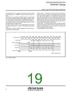
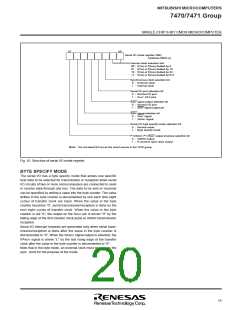
b7
b0
Serial I/O mode register (SM)
(Address 00DC16
)
Internal clock selection bits
00 : f(XIN) or f(XcIN) divided by 8
01 : f(XIN) or f(XcIN) divided by 16
10 : f(XIN) or f(XcIN) divided by 32
11 : f(XIN) or f(XcIN) divided by 512
Synchronous clock selection bit
0 : External clock
1 : Internal clock
Serial I/O port selection bit
0 : Normal I/O port
1 : SOUT, CLK pins
S
RDY signal output selection bit
0 : Normal I/O port
1 : SRDY signal output pin
S
RDY signal selection bit
0 : SRDY signal
1 : SARDY signal
Serial I/O byte specify mode selection bit
0 : Normal mode
1 : Byte specify mode
P15/SOUT, P17/SRDY output structure selection bit
0 : CMOS output
1 : N-channel open drain output
Note : Do not select f(XCIN) as the count source in the 7470 group.
Fig. 10 Structure of serial I/O mode register
BYTE SPECIFY MODE
The serial I/O has a byte specify mode that allows one specific
byte data to be selected for transmission or reception when serial
I/O circuits of two or more microcomputers are connected to send
or receive data through one bus. The data to be sent or received
can be specified by writing a value into the byte counter. The value
written in the byte counter is decremented by one each time eight
cycles of transfer clock are input. When the value in the byte
counter becomes “0”, serial transmission/reception is done by the
next eight cycles of transfer clock. When the value in the byte
counter is not “0”, the output on the SOUT pin is driven “H” by the
falling edge of the first transfer clock pulse to inhibit transmission/
reception.
Serial I/O interrupt requests are generated only when serial trans-
mission/reception is done after the value in the byte counter is
decremented to “0”. When the SARDY signal output is selected, the
SARDY signal is driven “L” by the last rising edge of the transfer
clock after the value in the byte counter is decremented to “0”.
Note that in the byte mode, an external clock must be used as the
sync. clock for the purpose of the mode.
19

 ETC [ ETC ]