MITSUBISHI MICROCOMPUTERS
7470/7471 Group
SINGLE-CHIP 8-BIT CMOS MICROCOMPUTER
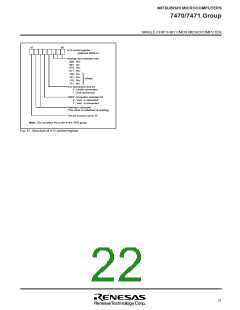
I/O PORTS
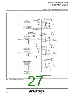
(4) Port P3
Port P3 is a 4-bit input port.
(5) Port P4
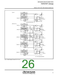
(1) Port P0
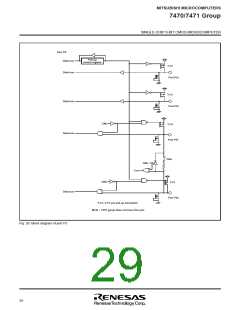
Port P0 is an 8-bit I/O port with CMOS outputs. As shown in
Figure 2, P0 can be accessed as memory through zero page
address 00C016. Port P0’s direction register allows each bit to
be programmed individually as input or output. The direction
register (zero page address 00C116) can be programmed as
input with “0”, or as output with “1”. When in the output mode,
the data to be output is latched to the port latch and output.
When data is read from the output port, the output pin level is
not read, only the latched data of the port latch is read. There-
fore, a previously output value can be read correctly even
though the output voltage level has been shifted up or down.
Port pins set as input are in the high impedance state so the
signal level can be read. When data is written into the input
port, the data is latched only to the output latch and the pin
still remains in the high impedance state. Following the ex-
ecution of STP or WIT instruction, key matrix with port P0 can
be used to generate the interrupt to bring the microcomputer
back in its normal state. When this port is selected for input,
pull-up transistor can be connected in units of 1-bit.
Port P4 is a 4-bit I/O port and has basically the same func-
tions as port P0. In the 7470 group, this port is P40 and P41,
a 2-bit I/O port. When this port is selected for input, pull-up
transistor can be connected in units of 4-bit .
(6) Port P5
Port P5 is a 4-bit input port and pull-up transistor can be con-
nected in units of 4-bit. P50 and P51 are shared with clock
generating circuit input/output pins.
The 7470 group does not have this port.
(7) INT0 pin (P30/INT0 pin)
This is an interrupt input pin, and is shared with port P30.
When “H” to “L” or “L” to “H” transition input is applied to this
pin, the INT0 interrupt request bit (bit 0 of address 00FD16) is
set to “1”.
(8) INT1 pin (P31/INT1 pin)
This is an interrupt input pin, and is shared with port P31.
When “H” to “L” or “L” to “H” transition input is applied to this
pin, the INT1 interrupt request bit (bit 1 of address 00FD16) is
set to “1”.
(2) Port P1
Port P1 has the same function as port P0. P12–P17 serve
dual functions, and the desired function can be selected by
the program. When this port is selected for input, pull-up tran-
sistor can be connected in units of 4-bit.
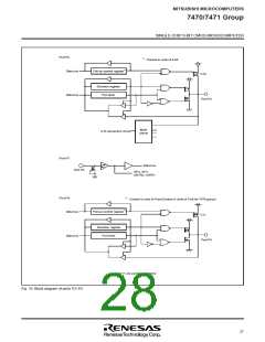
(9) Counter input CNTR0 pin (P32/CNTR0 pin)
This is a timer input pin, and is shared with port P32.
When this pin is selected to CNTR0 or CNTR1 interrupt input
pin and “H” to “L” or “L” to “H” transition input is applied to this
pin, the CNTR0 or CNTR1 interrupt request bit (bit 2 of ad-
dress 00FD16) is set to “1”.
(3) Port P2
Port P2 has the same function as port P0. In the 7470 group,
this port is P20–P23, a 4-bit I/O port. This port can also be
used as the analog voltage input pins. When this port is se-
lected for input, pull-up transistor can be connected in units of
4-bit.
(10) Counter input CNTR1 pin (P33/CNTR1 pin)
This is a timer input pin, and is shared with port P33.
When this pin is selected to CNTR0 or CNTR1 interrupt input
pin and “H” to “L” or “L” to “H” transition input is applied to this
pin, the CNTR0 or CNTR1 interrupt request bit (bit 2 of ad-
dress 00FD16) is set to “1”.
24

 ETC [ ETC ]