MITSUBISHI MICROCOMPUTERS
7470/7471 Group
SINGLE-CHIP 8-BIT CMOS MICROCOMPUTER
TIMER
The count source can be selected from the f(XIN) divided by 16,
f(XCIN) divided by 16, f(XCIN), timer 1 or timer 2 overflow, or an
event input from P33/CNTR1 pin according to the statuses of bit 1
and bit 2 in the timer 34 mode register, bit 6 in the timer mode reg-
ister 2 (address 00FA16) and bit 7 in the CPU mode register. Do
not select f(XCIN) as the count source in the 7470 group. Note,
however, that if timer 1 overflow or timer 2 overflow is selected for
the count source of timer 3 when timer 1 overflow is selected for
the count source of timer 2, timer 1 overflow is always selected re-
gardless of the status of bit 6 in the timer mode register 2. Event
inputs are selected depending on bit 3 in the edge polarity selec-
tion register. When this bit is “0”, the inverted value of CNTR1 input
is selected; when the bit is “1”, CNTR1 input is selected.
Timer 4 can be operated in the timer mode, event count mode,
pulse output mode, pulse width measuring mode, or PWM mode.
Timer 4 starts counting when bit 3 in the timer 34 mode register is
set to “0” when bit 6 in this register is “0”. When bit 6 is “1”, the
pulse width measuring mode is selected. The count source can be
selected from timer 3 overflow, f(XIN) divided by 16, f(XCIN) divided
by 16, f(XCIN), timer 1 or timer 2 overflow, or an event input from
P33/CNTR1 pin according to the statuses of bit 4 and bit 5 in the
timer 34 mode register, bit 6 in the timer mode register 2, and bit 7
in the CPU mode register. Do not select f(XCIN) as the count
source in the 7470 group. Note, however, that if timer 1 overflow or
timer 2 overflow is selected for the count source of timer 4 when
timer 1 overflow is selected for the count source of timer 2, timer 1
overflow is always selected regardless of the status of bit 6 in the
timer mode register 2. Event inputs are selected depending on bit
3 in the edge polarity selection register.
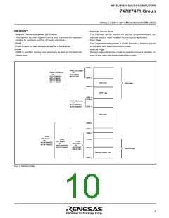
The 7470/7471 group has four timers; timer 1, timer 2, timer 3, and
timer 4.
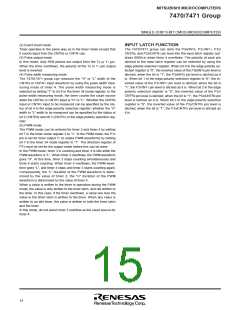
A block diagram of timer 1 through 4 is shown in Figure 6.
Timer 1 can be operated in the timer mode, event count mode, or
pulse output mode. Timer 1 starts counting when bit 0 in the timer
12 mode register (address 00F816) is set to “0”.
The count source can be selected from the f(XIN) divided by 16,
f(XCIN) divided by 16, f(XCIN), or event input from P32/CNTR0 pin.
Do not select f(XCIN) as the count source in the 7470 group. When
bit 1 and bit 2 in the timer 12 mode register are “0”, f(XIN) divided
by 16 or f(XCIN) divided by 16 is selected. Selection between f(XIN)
and f(XCIN) is done by bit 7 in the CPU mode register (address
00FB16). When bit 1 in the timer 12 mode register is “0” and bit 2
is “1”, f(XCIN) is selected. And, when bit 1 in the timer 12 mode
register is “1”, an event input from the CNTR0 pin is selected.
Event inputs are selected depending on bit 2 in the edge polarity
selection register (address 00D416). When this bit is “0”, the in-
verted value of CNTR0 input is selected; when the bit is “1”,
CNTR0 input is selected.
When bit 3 in the timer 12 mode register is set to “1”, the P12 pin
becomes timer output T0. When the direction register of P12 is set
for the output mode at this time, the timer 1 overflow divided by 2
is output from T0.
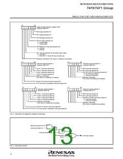
Please set the initial output value in the following procedure.
➀ Set “1” to bit 0 of the timer 12 mode register.
(Timer 1 count stop.)
➁ Set “1” to bit 0 of the timer mode register 2.
➂ Set the output value to bit 0 of the timer FF register.
➃ Set the count value to the timer 1.
When this bit is “0”, the inverted value of CNTR1 input is selected;
when the bit is “1”, CNTR1 input is selected.
➄ Set “0” to bit 0 of the timer 12 mode register.
(Timer 1 count start.)
When bit 7 in the timer 34 mode register is set to “1”, the P13 pin
becomes timer output T1. When the direction register of P13 is set
for the output mode at this time, the timer 4 overflow divided by 2
is output from T1 when bit 7 in the timer mode register 2 is “0”.
Please set the initial output value in the following procedure.
➀ Set “1” to bit 3 of the timer 34 mode register.
Timer 2 can only be operated in the timer mode. Timer 2 starts
counting when bit 4 in the timer 12 mode register is set to “0”.
The count source can be selected from the divide by 16, divide by
64, divide by 128, or divide by 256 frequency of f(XIN) or f(XCIN),
and timer 1 overflow. Do not select f(XCIN) as the count source in
the 7470 group. When bit 5 in the timer 12 mode register is “0”,
any of the divide by 16, divide by 64, divide by 128, or divide by
256 frequency of f(XIN) or (XCIN) is selected. The divide ratio is se-
lected according to bit 6 and bit 7 in the timer 12 mode register,
and selection between f(XIN) and f(XCIN) is made according to bit
7 in the CPU mode register. When bit 5 in the timer 12 mode reg-
ister is “1”, timer 1 overflow is selected as the count source.
Timer 3 can be operated in the timer mode, event count mode, or
PWM mode. Timer 3 starts counting when bit 0 in the timer 34
mode register (address 00F916) is set to “0”.
(Timer 4 count stop.)
➁ Set “1” to bit 1 of the timer mode register 2.
➂ Set the output value to bit 1 of the timer FF register.
➃ Set the count value to the timer 4.
➄ Set “0” to bit 3 of the timer 34 mode register.
(Timer 4 count start.)
(1) Timer mode
Timer performs down count operations with the dividing ratio being
1/(n+1). Writing a value to the timer latch sets a value to the timer.
When the value to be set to the timer latch is nn16, the value to be
set to a timer is nn16, which is down counted at the falling edge of
the count source from nn16 to (nn16-1) to (nn16-2) to ...0116 to
0016 to FF16. At the falling edge of the count source immediately
after timer value has reached FF16, value (nn16-1) obtained by
subtracting one from the timer latch value is set (reloaded) to the
timer to continue counting. At the rising edge of the count source
immediately after the timer value has reached FF16, an overflow
occurs and an interrupt request is generated.
13

 ETC [ ETC ]