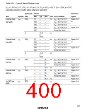
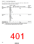
Table 15-3 Control Signal Timing (cont)
VCC = 1.8 V to 5.5 V, AVCC = 1.8 V to 5.5 V, VSS = AVSS = 0.0 V, Ta = –20°C to +75°C
(including subactive mode) unless otherwise indicated.
Applicable Values
Reference
Item
Symbol Pins
Min
Typ
Max
Unit Test Condition
Figure
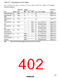
Input pin high
width
tIH
IRQ0 to
IRQ4,
2
—
—
tcyc
tsubcyc
Figure 15-3
WKP0 to
WKP7,
ADTRG,
TMIC
TMIF, TMIG,
AEVL,
AEVH
Input pin low
width
tIL
IRQ0 to
IRQ4,
2
—
—
tcyc
tsubcyc
Figure 15-3
WKP0 to
WKP7,
ADTRG,
TMIC, TMIF,
TMIG,
AEVL,
AEVH
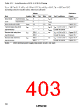
UD pin minimum tUDH
modulation width tUDL
UD
4
—
—
tcyc
tsubcyc
Figure 15-4
Notes: 1. Selected with SA1 and SA0 of system clock control register 2 (SYSCR2).
2. When internal power supply step-down circuit is not used.
386

 ETC [ ETC ]