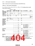
15.2.4
A/D Converter Characteristics
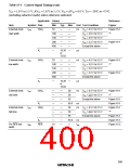
Table 15-6 shows the A/D converter characteristics of the H8/3887 Series.
Table 15-6 A/D Converter Characteristics
VCC = 1.8 V to 5.5 V, VSS = AVSS = 0.0 V, Ta = –20°C to +75°C (including subactive mode)
unless otherwise indicated.
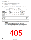
Applicable Values
Item
Symbol Pins
Min
Typ
Max
Unit
Test Condition
Notes
1
Analog power AVCC
supply voltage
AVCC
1.8
—
5.5
V
*
Analog input
voltage
AVIN
AN0 to AN11 – 0.3
—
AVCC + 0.3 V
Analog power AIOPE
AVCC
—
—
—
1.5
—
mA
AVCC = 5.0 V
2
supply current AISTOP1 AVCC
600
µA
*
Reference
value
3
AISTOP2 AVCC
—
—
—
—
5
µA
*
Analog input
capacitance
CAIN
AN0 to AN11
15.0
pF
Allowable
RAIN
—
—
10.0
kΩ
signal source
impedance
Resolution
(data length)
—
—
—
—
—
—
10
bit
4
Nonlinearity
error
±2.5
±5.5
LSB
AVCC = 3.0 to 5.5 V
VCC = 3.0 to 5.5 V
*
AVCC = 2.0 to 5.5 V
VCC = 2.0 to 5.5 V
5
—
—
—
—
±7.5
±0.5
Except the above
*
Quantization
error
LSB
LSB
4
Absolute
accuracy
—
—
—
—
±3.0
±6.0
AVCC = 3.0 to 5.5 V
VCC = 3.0 to 5.5 V
*
AVCC = 2.0 to 5.5 V
VCC = 2.0 to 5.5 V
5
—
—
—
±8.0
Except the above
*
4
Conversion
time
15.5
155
µs
AVCC = 3.0 to 5.5 V
VCC = 3.0 to 5.5 V
*
62
—
155
Except the above
Notes: 1. Set AVCC = VCC when the A/D converter is not used.
2. AISTOP1 is the current in active and sleep modes while the A/D converter is idle.
3. AISTOP2 is the current at reset and in standby, watch, subactive, and subsleep modes
while the A/D converter is idle.
4. When internal power supply step-down circuit is not used.
5. Conversion time: 124 µs
389

 ETC [ ETC ]