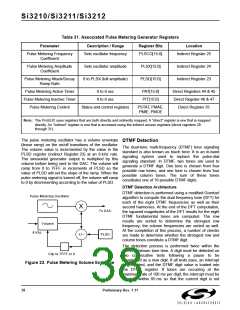
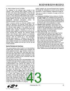
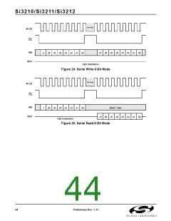
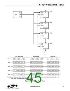
Si3210/Si3211/Si3212
receive path.
The ProSLIC also provides a means to compensate for
degraded subscriber loop conditions involving
excessive line capacitance (leakage). The CLC[1:0] bits
of direct Register 10 increase the ac signal magnitude
to compensate for the additional loss at the high end of
the audio frequency range. The default setting of
CLC[2:0] assumes no line capacitance.
An additional analog loopback (ALM1) takes the
digital stream at the output of the A/D converter and
feeds it back to the D/A converter. (See Figure 23.)
The signal path starts with the analog signal at the
input of the transmit path and ends with an analog
signal at the output of the receive path. This
loopback option allows the testing of the analog
signal processing circuitry of the Si3210 completely
independent from any activity in the DSP.
Silicon revisions C and higher support the option to
remove the internal reference resistor used to
synthesize ac impedances for 600 + 2.16 µF and
900 + 2.16 µF settings so that an external resistor
reference may be used. This option is enabled by
setting ZSEXT = 1 (direct Register 108, bit 4).
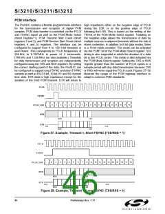
The full digital loopback tests almost all the circuitry
of both the transmit and receive paths. The analog
signal at the output of the receive path is fed back to
the input of the transmit path by way of the hybrid
filter path. (See Figure 23.) The signal path starts
with 8-bit PCM data input to the receive path and
ends with 8-bit PCM data at the output of the
Clock Generation
The ProSLIC will generate the necessary internal clock
frequencies from the PCLK input. PCLK must be
synchronous to the 8 kHz FSYNC clock and run at one
of the following rates: 256 kHz, 512 kHz, 768 kHz,
transmit path. The user can bypass the companding
process and interface directly to the 16-bit data.
An additional digital loopback (DLM) takes the digital 1.024 MHz, 1.536 MHz, 2.048 MHz, 4.096 MHz or
stream at the input of the D/A converter in the
receive path and feeds it back to the transmit A/D
digital filter. The signal path starts with 8-bit PCM
data input to the receive path and ends with 8-bit
PCM data at the output of the transmit path. This
loopback option allows the testing of the digital
signal processing circuitry of the Si3210 completely
independent from any analog signal processing
activity.The user can bypass the companding
process and interface directly to the 16-bit data.
8.192 MHz. The ratio of the PCLK rate to the FSYNC
rate is determined via a counter clocked by PCLK. The
three-bit ratio information is automatically transferred
into an internal register, PLL_MULT, following a reset of
the ProSLIC. The PLL_MULT is used to control the
internal PLL which multiplies PCLK as needed to
generate 16.384 MHz rate needed to run the internal
filters and other circuitry.
The PLL clock synthesizer settles very quickly following
power up. However, the settling time depends on the
PCLK frequency and it can be approximately predicted
by the following equation:
Two-Wire Impedance Matching
The ProSLIC provides on-chip programmable two-wire
impedance settings to meet a wide variety of worldwide
two-wire return loss requirements. The two-wire
impedance is programmed by loading one of the eight
available impedance values into the TISS[2:0] bits of the
Two-Wire Impedance Synthesis Control register (direct
Register 10). If direct Register 10 is not user-defined,
the default setting of 600 Ω will be loaded into the TISS
register.
64
FPCLK
----------------
=
TSETTLE
Interrupt Logic
The ProSLIC is capable of generating interrupts for the
following events:
Loop current/ring ground detected
Ring trip detected
Real and complex two-wire impedances are realized by
internal feedback of a programmable amplifier (RAC) a
Power alarm
DTMF digit detected (Si3210 and Si3211 only)
Active timer 1 expired
switched
capacitor
network
(XAC)
and
a
transconductance amplifier (G ). (See Figure 23.) RAC
m
Inactive timer 1 expired
creates the real portion and XAC creates the imaginary
portion of G ’s input. G then creates a current that
Active timer 2 expired
m
m
models the desired impedance value to the subscriber
loop. The differential ac current is fed to the subscriber
loop via the ITIPP and IRINGP pins through an off-chip
Inactive timer 2 expired
Ringing active timer expired
Ringing inactive timer expired
Pulse metering active timer expired
Pulse metering inactive timer expired
current buffer (I
), which is implemented using
BUF
transistor Q1 and Q2 (see Figure on page 16). G is
m
referenced to an off-chip resistor (R ).
15
42
Preliminary Rev. 1.11

 ETC [ ETC ]