Si3210/Si3211/Si3212
Receive Path
should be interpreted as the maximum allowable
magnitude of any spurious signals that are generated
when a PCM data stream representing a sine wave
signal in the range of 300 Hz to 3.4 kHz at a level of
0 dBm0 is applied at the digital input.
In the receive path, the optionally compressed 8-bit data
is first expanded to 16-bit words. The PCMF register bit
can bypass the expansion process, in which case two
8-bit words are assembled into one 16-bit word. DACG
is the receive path programmable gain amplifier which The group delay distortion in either path is limited to no
can be programmed from –∞ dB to 6 dB. An 8 kHz, 16- more than the levels indicated in Figure 5 on page 10.
bit signal is then provided to a D/A converter. The The reference in Figure 5 is the smallest group delay for
resulting analog signal is amplified by the analog a sine wave in the range of 500 Hz to 2500 Hz at
receive amplifier, ARX, which is user selectable to one 0 dBm0.
of mute/–3.5/0/3.5 dB options. It is then applied at the
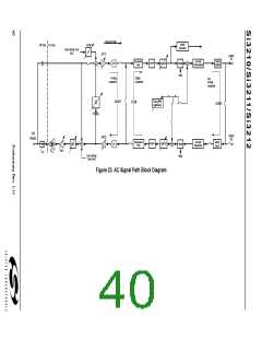
The block diagram for the voice-band signal processing
input of the transconductance amplifier (Gm) which
paths are shown in Figure 23. Both the receive and the
drives the off-chip current buffer (I
).
BUF
transmit paths employ the optimal combination of
analog and digital signal processing to provide the
maximum performance while, at the same time, offering
sufficient flexibility to allow users to optimize for their
particular application of the ProSLIC. All programmable
signal-processing blocks are symbolically indicated in
Figure 23 by a dashed arrow across them. The two-wire
(TIP/RING) voice-band interface to the ProSLIC is
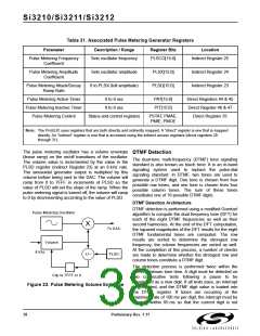
Audio Characteristics
The dominant source of distortion and noise in both the
transmit and receive paths is the quantization noise
introduced by the µ-law or the A-law compression
process. Figure 1 on page 7 specifies the minimum
signal-to-noise-and-distortion ratio for either path for a
sine wave input of 200 Hz to 3400 Hz.
implemented using
components. The receive path interface consists of a
unity-gain current buffer, I , while the transmit path
a small number of external
Both the µ-law and the A-law speech encoding allow the
audio codec to transfer and process audio signals larger
than 0 dBm0 without clipping. The maximum PCM code
is generated for a µ-law encoded sine wave of
3.17 dBm0 or an A-law encoded sine wave of
3.14 dBm0. The ProSLIC overload clipping limits are
driven by the PCM encoding process. Figure 2 on page
BUF
interface is simply an ac coupling capacitor. Signal
paths, although implemented differentially, are shown
as single-ended for simplicity.
Transhybrid Balance
7 shows the acceptable limits for the analog-to-analog The ProSLIC provides programmable transhybrid
fundamental power transfer-function, which bounds the balance with gain block H. (See Figure 23.) In the ideal
behavior of ProSLIC.
case where the synthesized SLIC impedance matches
exactly the subscriber loop impedance, the transhybrid
balance should be set to subtract a –6 dB level from the
transmit path signal. The transhybrid balance gain can
be adjusted from –2.77 dB to +4.08 dB around the ideal
setting of –6 dB by programming the HYBA[2:0] bits of
the Hybrid Control register (direct Register 11). Note
that adjusting any of the analog or digital gain blocks will
not require any modification of the transhybrid balance
gain block, as the transhybrid gain is subtracted from
the transmit path signal prior to any gain adjustment
stages. The transhybrid balance can also be disabled, if
desired, using the appropriate register setting.
The transmit path gain distortion versus frequency is
shown in Figure 3 on page 8. The same figure also
presents the minimum required attenuation for any out-
of-band analog signal that may be applied on the line.
Note the presence of a high-pass filter transfer-function,
which ensures at least 30 dB of attenuation for signals
below 65 Hz. The low-pass filter transfer function which
attenuates signals above 3.4 kHz has to exceed the
requirements specified by the equations in Figure 3 on
page 8 and it is implemented as part of the A-to-D
converter.
The receive path transfer function requirement, shown
in Figure 4 on page 9, is very similar to the transmit path Loopback Testing
transfer function. The most notable difference is the
Four loopback test options are available in the ProSLIC:
absence of the high-pass filter portion. The only other
differences are the maximum 2 dB attenuation at
200 Hz (as opposed to 3 dB for the transmit path) and
the 28 dB of attenuation for any frequency above
4.6 kHz. The PCM data rate is 8 kHz and thus, no
frequencies greater than 4 kHz can be digitally encoded
in the data stream. From this point of view, at
frequencies greater than 4 kHz, the plot in Figure 4
The full analog loopback (ALM2) tests almost all the
circuitry of both the transmit and receive paths. The
compressed 8-bit word transmit data stream is fed
back serially to input of the receive path expander.
(See Figure 23.) The signal path starts with the
analog signal at the input of the transmit path and
ends with an analog signal at the output of the
Preliminary Rev. 1.11
41

 ETC [ ETC ]