Si3210/Si3211/Si3212
Indirect register access complete
Indirect registers are accessed through direct registers
29 through 30. Instructions on how to access them is
described in “Control Registers” beginning on page 50.
The interface to the interrupt logic consists of six
registers. Three interrupt status registers contain 1 bit
for each of the above interrupt functions. These bits will
be set when an interrupt is pending for the associated
resource. Three interrupt enable registers also contain 1
bit for each interrupt function. In the case of the interrupt
enable registers, the bits are active high. Refer to the
There are a number of variations of usage on this four-
wire interface:
Continuous clocking. During continuous clocking,
the data transfers are controlled by the assertion of
the CS pin. CS must assert before the falling edge of
SCLK on which the first bit of data is expected during
a read cycle, and must remain low for the duration of
the 8 bit transfer (command/address or data).
appropriate
functional
description
section
for
operational details of the interrupt functions.
When a resource reaches an interrupt condition, it will
signal an interrupt to the interrupt control block. The
interrupt control block will then set the associated bit in
the interrupt status register if the enable bit for that
interrupt is set. The INT pin is a NOR of the bits of the
interrupt status registers. Therefore, if a bit in the
interrupt status registers is asserted, IRQ will assert low.
Upon receiving the interrupt, the interrupt handler
should read interrupt status registers to determine
which resource is requesting service. To clear a pending
interrupt, write the desired bit in the appropriate
interrupt status register to 1. Writing a 0 has no effect.
This provides a mechanism for clearing individual bits
when multiple interrupts occur simultaneously. While the
interrupt status registers are non-zero, the INT pin will
remain asserted.
SDI/SDO wired operation. Independent of the
clocking options described, SDI and SDO can be
treated as two separate lines or wired together if the
master is capable of tristating its output during the
data byte transfer of a read operation.
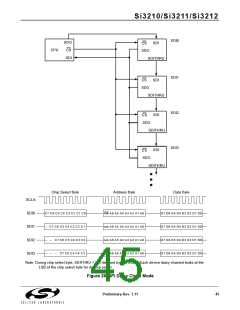
Daisy chain mode. This mode allows
communication with banks of up to eight ProSLIC
devices using one chip select signal. When the
SPIDC bit in the SPI Mode Select register is set,
data transfer mode changes to a 3-byte operation: a
chip select byte, an address/control byte, and a data
byte. Using the circuit shown in Figure 26, a single
device may select from the bank of devices by
setting the appropriate chip select bit to a one. Each
device uses the LSB of the chip select byte, shifts
the data right by one bit, and passes the chip select
byte using the SDITHRU pin to the next device in the
chain. Address/control and data bytes are unaltered.
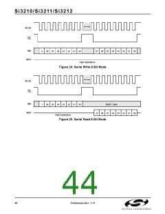
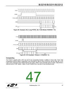
Serial Peripheral Interface
The control interface to the ProSLIC is a 4-wire interface
modeled after commonly available micro-controller and
serial peripheral devices. The interface consists of a
clock (SCLK), chip select (CS), serial data input (SDI),
and serial data output (SDO). Data is transferred a byte
at a time with each register access consisting of a pair
of byte transfers. Figures 24 and 25 illustrate read and
write operation in the SPI bus.
The first byte of the pair is the command/address byte.
The MSB of this byte indicates register read when 1 and
a register write when 0. The remaining seven bits of the
command/address byte indicate the address of the
register to be accessed. The second byte of the pair is
the data byte. During a read operation, the SDO
becomes active and the 8-bit contents of the register
are driven out MSB first. The SDO will be high
impedence on either the falling edge of SCLK following
the LSB, or the rising of CS whichever comes first. SDI
is a “don’t care” during the data portion of read
operations. During write operations, data is driven into
the ProSLIC via the SDI pin MSB first. The SDO pin will
remain high impedance during write operations. Data
always transitions with the falling edge of the clock and
is latched on the rising edge. The clock should return to
a logic high when no transfer is in progress.
Preliminary Rev. 1.11
43

 ETC [ ETC ]