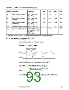
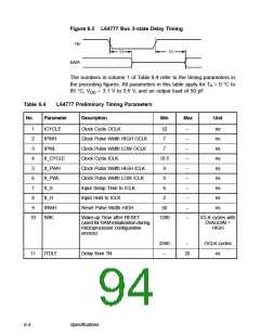
Figure 6.3 L64777 Bus 3-state Delay Timing
TN
11
11
DATA
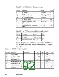
The numbers in column 1 of Table 6.4 refer to the timing parameters in
the preceding figures. All parameters in this table apply for T = 0 °C to
A
85 °C, V
= 3.1 V to 3.6 V, and an output load of 50 pF.
DD
Table 6.4
L64777 Preliminary Timing Parameters
Description
No.
Parameter
tCYCLE
Min
Max
Unit
1
Clock Cycle OCLK
32
7
–
–
–
–
–
–
–
–
–
–
ns
ns
ns
ns
ns
ns
ns
ns
ns
2
3
tPWH
tPWL
Clock Pulse Width HIGH OCLK
Clock Pulse Width LOW OCLK
Clock Cycle ICLK
7
4
tI_CYCLE
tI_PWH
tI_PWL
tI_S
18.5
9
5
Clock Pulse Width HIGH ICLK
Clock Pulse Width LOW ICLK
Input Setup Time to ICLK
Input Hold to ICLK
6
9
7
6
8
tI_H
2
9
tRWH
tWK
Reset Pulse Width HIGH
50
1280
10
Wake-up Time after RESET
(used for RAM initialization during
microprocessor configuration
access)
ICLK cycles with
DVALIDIN =
HIGH
2560
–
–
OCLK cycles
ns
11
tTDLY
Delay from TN
20
6-4
Specifications

 ETC [ ETC ]