Table 6.3
L64777 DC Characteristics (Cont.)
Symbol Parameter
Condition1
Min
Typ
Max
Units
IIN
IIN
IIN
Input Current Leakage
VDD = Max, VIN
VDD or VSS
=
=
=
−10
± 1
10
mA
Input Current Leakage
w/Pullup
VDD = Max, VIN
VDD or VSS
−62
−62
−215
−215
−384
−384
2
mA
mA
Input Current Leakage
w/Pulldown
VDD = Max, VIN
VDD or VSS
IDD
ICC
Quiescent Supply Current VIN = VDD or VSS
mA
mA
Dynamic Supply Current
ICLK = 54 MHz max,
PLL MODE 2 PCLK
90 MHz
50
VDD = Max
1. Specified at VDD = 3.3 V ± 5% at ambient temperature over the specified range.
6.1.2 AC Timing Diagrams for L64777
Figure 6.1 illustrates the TS input timing.
Figure 6.1 TS Input Timing
1 & 4
2 & 5
3 & 6
ICLK
7
8
Inputs
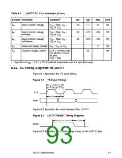
Figure 6.2 illustrates the reset timing of the L64777.
Figure 6.2 L64777 RESET Timing Diagram
9
10
RESET
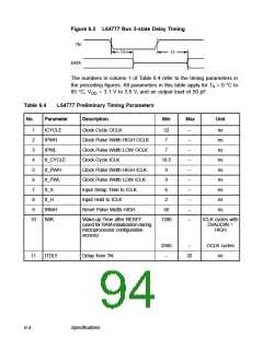
Figure 6.3 illustrates the 3-state delay timing of the L64777 bus.
AC/DC Specifications
6-3

 ETC [ ETC ]