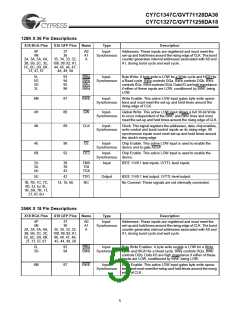
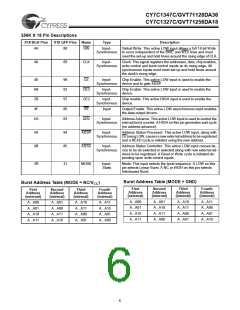
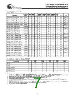
CY7C1347C/GVT71128DA36
CY7C1327C/GVT71256DA18
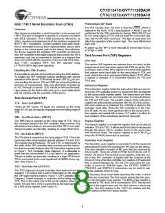
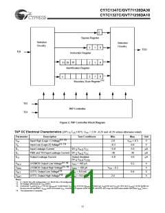
Identification (ID) Register
ture-DR mode and places the ID register between the TDI and
TDO pins in Shift-DR mode. The IDCODE instruction is the
default instruction loaded in the instruction upon power-up and
at any time the TAP controller is placed in the test-logic reset
state.
The ID Register is a 32-bit register that is loaded with a device
and vendor specific 32-bit code when the controller is put in
Capture-DR state with the IDCODE command loaded in the
instruction register. The register is then placed between the
TDI and TDO pins when the controller is moved into Shift-DR
state. Bit 0 in the register is the LSB and the first to reach TDO
when shifting begins. The code is loaded from a 32-bit on-chip
ROM. It describes various attributes of the device as described
in the Identification Register Definitions table.
SAMPLE-Z
If the High-Z instruction is loaded in the instruction register, all
output pins are forced to a High-Z state and the boundary scan
register is connected between TDI and TDO pins when the
TAP controller is in a Shift-DR state.
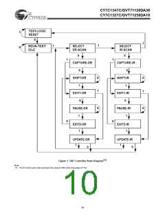
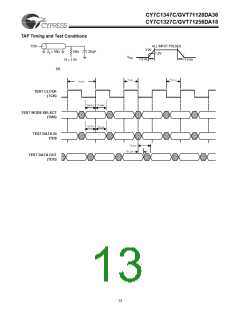
TAP Controller Instruction Set
SAMPLE/PRELOAD
Overview
SAMPLE/PRELOAD is an IEEE 1149.1 mandatory instruction.
The PRELOAD portion of the command is not implemented in
this device, so the device TAP controller is not fully IEEE
1149.1-compliant.
There are two classes of instructions defined in the IEEE Stan-
dard 1149.1-1990; the standard (public) instructions and de-
vice specific (private) instructions. Some public instructions
are mandatory for IEEE 1149.1 compliance. Optional public
instructions must be implemented in prescribed ways.
When the SAMPLE/PRELOAD instruction is loaded in the in-
struction register and the TAP controller is in the Capture-DR
state, a snap shot of the data in the device’s input and I/O
buffers is loaded into the boundary scan register. Because the
device system clock(s) are independent from the TAP clock
(TCK), it is possible for the TAP to attempt to capture the input
and I/O ring contents while the buffers are in transition (i.e., in
a metastable state). Although allowing the TAP to sample
metastable inputs will not harm the device, repeatable results
can not be expected. To guarantee that the boundary scan
register will capture the correct value of a signal, the device
input signals must be stabilized long enough to meet the TAP
Although the TAP controller in this device follows the IEEE
1149.1 conventions, it is not IEEE 1149.1 compliant because
some of the mandatory instructions are not fully implemented.
The TAP on this device may be used to monitor all input and
I/O pads, but can not be used to load address, data, or control
signals into the device or to preload the I/O buffers. In other
words, the device will not perform IEEE 1149.1 EXTEST, IN-
TEST, or the preload portion of the SAMPLE/PRELOAD com-
mand.
When the TAP controller is placed in Capture-IR state, the two
least significant bits of the instruction register are loaded with
01. When the controller is moved to the Shift-IR state the in-
struction is serially loaded through the TDI input (while the
previous contents are shifted out at TDO). For all instructions,
the TAP executes newly loaded instructions only when the con-
troller is moved to Update-IR state. The TAP instruction sets
for this device are listed in the following tables.
controller’s capture setup plus hold time (t
plus t ). The
CS
CH
device clock input(s) need not be paused for any other TAP
operation except capturing the input and I/O ring contents into
the boundary scan register.
Moving the controller to Shift-DR state then places the bound-
ary scan register between the TDI and TDO pins. Because the
PRELOAD portion of the command is not implemented in this
device, moving the controller to the Update-DR state with the
SAMPLE/PRELOAD instruction loaded in the instruction reg-
ister has the same effect as the Pause-DR command.
EXTEST
EXTEST is an IEEE 1149.1 mandatory public instruction. It is
to be executed whenever the instruction register is loaded with
all 0s. EXTEST is not implemented in this device.
BYPASS
When the BYPASS instruction is loaded in the instruction reg-
ister and the TAP controller is in the Shift-DR state, the bypass
register is placed between TDI and TDO. This allows the board
level scan path to be shortened to facilitate testing of other
devices in the scan path.
The TAP controller does recognize an all-0 instruction. When
an EXTEST instruction is loaded into the instruction register,
the device responds as if a SAMPLE/PRELOAD instruction
has been loaded. There is one difference between two instruc-
tions. Unlike SAMPLE/PRELOAD instruction, EXTEST places
the device outputs in a High-Z state.
Reserved
Do not use these instructions. They are reserved for future
use.
IDCODE
The IDCODE instruction causes a vendor-specific, 32-bit code
to be loaded into the ID register when the controller is in Cap-
9

 ETC [ ETC ]