CY7C1347C/GVT71128DA36
CY7C1327C/GVT71256DA18
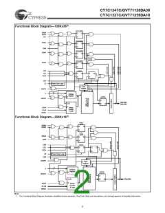
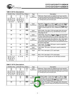
128K X 36 Pin Descriptions
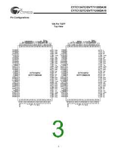
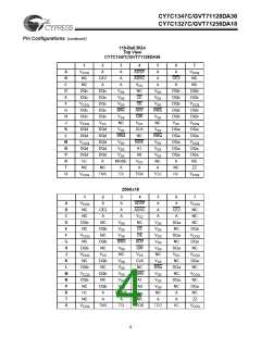
X36 BGA Pins
X36 QFP Pins Name
Type
Description
4P
4N
37
36
A0
A1
A
Input-
Addresses: These inputs are registered and must meet the
Synchronous set-up and hold times around the rising edge of CLK. The burst
counter generates internal addresses associated with A0 and
A1, during burst cycle and wait cycle.
2A, 3A, 5A, 6A,
3B, 5B, 2C, 3C, 100, 99, 82, 81,
35, 34, 33, 32,
5C, 6C, 2R, 6R,
3T, 4T, 5T
44, 45, 46, 47,
48, 49, 50
5L
5G
3G
3L
93
94
95
96
BWa
BWb
BWc
BWd
Input-
Byte Write: A byte write is LOW for a Write cycle and HIGH for
Synchronous a Read cycle. BWa controls DQa. BWb controls DQb. BWc
controls DQc. BWd controls DQd. Data I/O are high impedance
if either of these inputs are LOW, conditioned by BWE being
LOW.
4M
4H
4K
87
88
89
BWE
GW
Input-
Write Enable: This active LOW input gates byte write opera-
Synchronous tions and must meet the set-up and hold times around the
rising edge of CLK.
Input-
Global Write: This active LOW input allows a full 36-bit Write
Synchronous to occur independent of the BWE and BWn lines and must
meet the set-up and hold times around the rising edge of CLK.
CLK
Input-
Clock: This signal registers the addresses, data, chip enables,
Synchronous write control and burst control inputs on its rising edge. All
synchronous inputs must meet set-up and hold times around
the clock’s rising edge.
4E
6B
98
92
CE
Input-
Chip Enable: This active LOW input is used to enable the
Synchronous device and to gate ADSP.
CE2
Input-
Chip Enable: This active LOW input is used to enable the
Synchronous device.
2U
3U
4U
38
39
43
TMS
TDI
TCK
Input
IEEE 1149.1 test inputs. LVTTL-level inputs.
5U
42
TDO
NC
Output
-
IEEE 1149.1 test output. LVTTL-level output.
1B, 7B, 1C, 7C,
4D, 3J, 5J, 4L,
1R, 5R, 7R, 1T,
2T, 6T, 6U
14, 16, 66
No Connect: These signals are not internally connected.
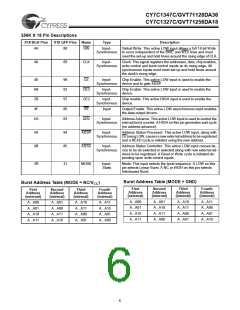
256K X 18 Pin Descriptions
X18 BGA Pins
X18 QFP Pins Name
Type
Description
4P
4N
37
36
A0
A1
A
Input-
Addresses: These inputs are registered and must meet the
Synchronous set-up and hold times around the rising edge of CLK. The burst
counter generates internal addresses associated with A0 and
A1, during burst cycle and wait cycle.
2A, 3A, 5A, 6A,
3B, 5B, 2C, 3C, 100, 99, 82, 81,
35, 34, 33, 32,
5C, 6C, 2R, 6R,
2T, 3T, 5T, 6T
80, 48, 47, 46,
45, 44, 49, 50
5L
3G
93
94
BWa
BWb
Input-
Byte Write Enables: A byte write enable is LOW for a Write
Synchronous cycle and HIGH for a Read cycle. BWa controls DQa. BWb
controls DQb. Data I/O are high impedance if either of these
inputs are LOW, conditioned by BWE being LOW.
4M
87
BWE
Input-
Write Enable: This active LOW input gates byte write opera-
Synchronous tions and must meet the setup and hold times around the rising
edge of CLK.
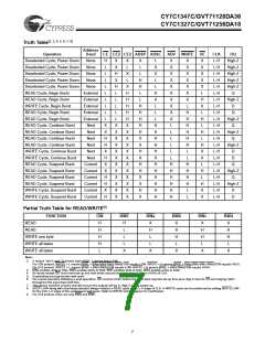
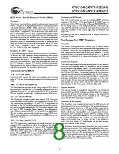
5

 ETC [ ETC ]