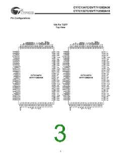
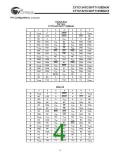
CY7C1347C/GVT71128DA36
CY7C1327C/GVT71256DA18
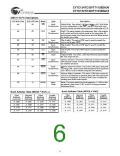
Truth Table[2, 3, 4, 5, 6, 7, 8]
Address
Used
Operation
CE CE2 CE2 ADSP ADSC
ADV
X
X
X
X
X
X
X
X
X
X
L
WRITE OE
CLK
L-H
L-H
L-H
L-H
L-H
L-H
L-H
L-H
L-H
L-H
L-H
L-H
L-H
L-H
L-H
L-H
L-H
L-H
L-H
L-H
L-H
L-H
DQ
High-Z
High-Z
High-Z
High-Z
High-Z
Q
Deselected Cycle, Power Down
Deselected Cycle, Power Down
Deselected Cycle, Power Down
Deselected Cycle, Power Down
Deselected Cycle, Power Down
READ Cycle, Begin Burst
None
None
H
L
X
X
H
X
H
L
X
L
X
L
L
X
X
L
X
X
X
X
X
X
X
L
X
X
X
X
X
L
None
L
X
L
L
None
L
H
H
L
None
L
X
H
H
H
H
H
X
X
X
X
X
X
X
X
X
X
X
X
L
External
External
External
External
External
Next
L
X
X
L
READ Cycle, Begin Burst
L
L
L
H
X
L
High-Z
D
WRITE Cycle, Begin Burst
READ Cycle, Begin Burst
L
L
H
H
H
H
H
X
X
H
X
H
H
X
X
H
X
L
L
L
H
H
H
H
H
H
L
Q
READ Cycle, Begin Burst
L
L
L
H
L
High-Z
Q
READ Cycle, Continue Burst
READ Cycle, Continue Burst
READ Cycle, Continue Burst
READ Cycle, Continue Burst
WRITE Cycle, Continue Burst
WRITE Cycle, Continue Burst
READ Cycle, Suspend Burst
READ Cycle, Suspend Burst
READ Cycle, Suspend Burst
READ Cycle, Suspend Burst
WRITE Cycle, Suspend Burst
WRITE Cycle, Suspend Burst
X
X
H
H
X
H
X
X
H
H
X
H
X
X
X
X
X
X
X
X
X
X
X
X
H
H
H
H
H
H
H
H
H
H
H
H
Next
L
H
L
High-Z
Q
Next
L
Next
L
H
X
X
L
High-Z
D
Next
L
Next
L
L
D
Current
Current
Current
Current
Current
Current
H
H
H
H
H
H
H
H
H
H
L
Q
H
L
High-Z
Q
H
X
X
High-Z
D
L
D
Partial Truth Table for READ/WRITE[9]
FUNCTION
GW
H
BWE
BWa
BWb
BWc
X
BWd
READ
READ
H
L
L
L
X
X
H
L
X
H
H
L
X
H
H
L
H
H
WRITE one byte
WRITE all bytes
H
H
H
L
L
WRITE all bytes
L
X
X
X
X
Note:
2. X means “don’t care.” H means logic HIGH. L means logic LOW.
For X36 product, WRITE = L means [BWE + BWa*BWb*BWc*BWd]*GW equals LOW. WRITE = H means [BWE + BWa*BWb*BWc*BWd]*GW equals HIGH.
For X18 product, WRITE = L means [BWE + BWa*BWb]*GW equals LOW. WRITE = H means [BWE + BWa*BWb]*GW equals HIGH.
3. BWa enables write to DQa. BWb enables write to DQb. BWc enables write to DQc. BWd enables write to DQd.
4. All inputs except OE must meet set-up and hold times around the rising edge (LOW to HIGH) of CLK.
5. Suspending burst generates wait cycle.
6. For a write operation following a read operation, OE must be HIGH before the input data required set-up time plus High-Z time for OE and staying HIGH
throughout the input data hold time.
7. This device contains circuitry that will ensure the outputs will be in High-Z during power-up.
8. ADSP LOW along with chip being selected always initiates a READ cycle at the L-H edge of CLK. A WRITE cycle can be performed by setting WRITE LOW
for the CLK L-H edge of the subsequent wait cycle. Refer to WRITE timing diagram for clarification.
9. For X18 product, there are only BWa and BWb.
7

 ETC [ ETC ]