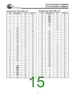
CY7C1347C/GVT71128DA36
CY7C1327C/GVT71256DA18
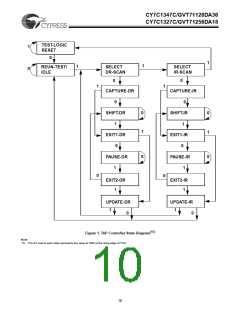
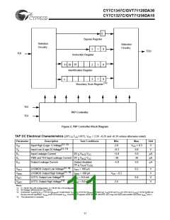
0
Bypass Register
Selection
Circuitry
Selection
Circuitry
2
1
0
TDO
TDI
Instruction Register
29
Identification Register
31 30
.
.
2
1
1
0
0
.
x
.
.
.
2
[11]
Boundary Scan Register
TDI
TDI
TAP Controller
Figure 2. TAP Controller Block Diagram
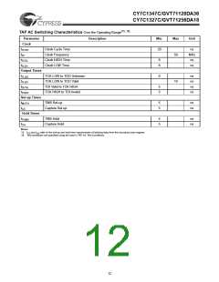
TAP DC Electrical Characteristics (20°C < T < 110°C; V = 3.3V –0.2V and +0.3V unless otherwise noted)
j
CC
Parameter
Description
Test Conditions
Min.
2.0
Max.
+ 0.3
CC
Unit
[12, 13]
V
V
Input High (Logic 1) Voltage
V
V
IH
Il
[12, 13]
Input Low (Logic 0) Voltage
Input Leakage Current
–0.3
–5.0
–30
0.8
5.0
30
V
IL
0V < V < V
µA
µA
µA
I
IN
CC
CC
IL
TMS and TDI Input Leakage Current 0V < V < V
IN
I
IL
Output Leakage Current
Output disabled,
0V < V < V
–5.0
5.0
O
IN
CCQ
[12, 14]
[12, 14]
V
LVCMOS Output Low Voltage
I
I
I
I
= 100 µA
0.2
0.4
V
V
V
V
OLC
OLC
OHC
OLT
V
LVCMOS Output High Voltage
= 100 µA
= 8.0 mA
= 8.0 mA
V
– 0.2
CC
OHC
[12]
V
LVTTL Output Low Voltage
OLT
[12]
V
LVTTL Output High Voltage
2.4
OHT
OHT
Notes:
11. X = 69 for the x36 configuration. X = 50 for the x18 configuration.
12. All Voltage referenced to VSS (GND).
13. Overshoot: VIH(AC)<VCC+1.5V for t<tKHKH/2, Undershoot: VIL(AC)<–0.5V for t<tKHKH/2, Power-up: VIH<3.6V and VCC<3.135V and VCCQ<1.4V for t<200 ms.
During normal operation, VCCQ must not exceed VCC. Control input signals (such as R/W, ADV/LD, etc.) may not have pulse widths less than tKHKL (min.).
14. This parameter is sampled.
11

 ETC [ ETC ]