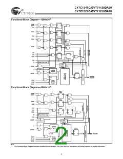
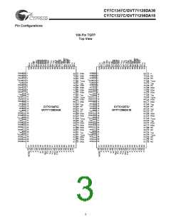
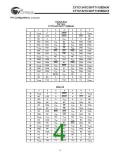
CY7C1347C/GVT71128DA36
CY7C1327C/GVT71256DA18
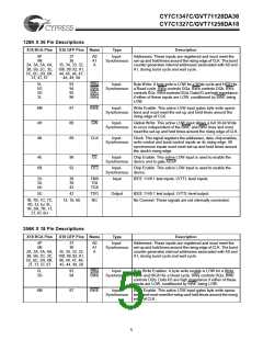
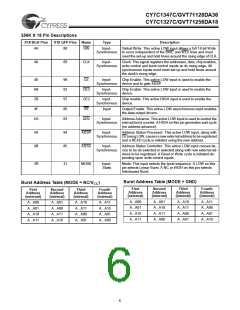
256K X 18 Pin Descriptions
X18 BGA Pins
X18 QFP Pins Name
Type
Description
4H
88
GW
Input-
Global Write: This active LOW input allows a full 18-bit Write
Synchronous to occur independent of the BWE and WEn lines and must
meet the set-up and hold times around the rising edge of CLK.
4K
89
CLK
Input-
Clock: This signal registers the addresses, data, chip enables,
Synchronous write control and burst control inputs on its rising edge. All
synchronous inputs must meet set-up and hold times around
the clock’s rising edge.
4E
6B
2B
4F
4G
98
92
97
86
83
CE
CE2
CE2
OE
Input-
Chip Enable: This active LOW input is used to enable the
Synchronous device and to gate ADSP.
Input-
Chip Enable: This active LOW input is used to enable the
Synchronous device.
input-
Chip enable: This active HIGH input is used to enable the
Synchronous device.
Input
Output Enable: This active LOW asynchronous input enables
the data output drivers.
ADV
Input-
Address Advance: This active LOW input is used to control the
Synchronous internal burst counter. A HIGH on this pin generates wait cycle
(no address advance).
4A
4B
84
85
ADSP
ADSC
Input-
Address Status Processor: This active LOW input, along with
Synchronous CE being LOW, causes a new external address to be registered
and a READ cycle is initiated using the new address.
Input-
Address Status Controller: This active LOW input causes de-
Synchronous vice to be de-selected or selected along with new external ad-
dress to be registered. A Read or Write cycle is initiated de-
pending upon write control inputs.
3R
31
MODE
Input-
Static
Mode: This input selects the burst sequence. A LOW on this
pin selects Linear Burst. A NC or HIGH on this pin selects
Interleaved Burst.
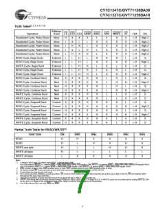
Burst Address Table (MODE = GND)
Burst Address Table (MODE = NC/V
)
CC
First
Address
(external)
Second
Address
(internal)
Third
Address
(internal)
Fourth
Address
(internal)
First
Address
(external)
Second
Address
(internal)
Third
Address
(internal)
Fourth
Address
(internal)
A...A00
A...A01
A...A10
A...A11
A...A01
A...A10
A...A11
A...A00
A...A10
A...A11
A...A00
A...A01
A...A11
A...A00
A...A01
A...A10
A...A00
A...A01
A...A10
A...A11
A...A01
A...A00
A...A11
A...A10
A...A10
A...A11
A...A00
A...A01
A...A11
A...A10
A...A01
A...A00
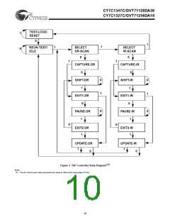
6

 ETC [ ETC ]