AN-32
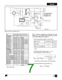
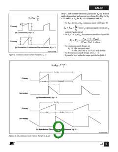
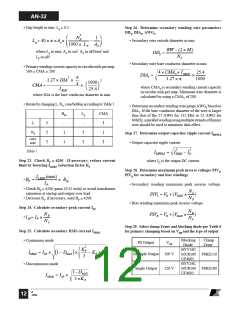
Step 4. Determine reflected output voltage VOR and clamp
Zener voltage VCLO (Figure 8)
TOPSwitch-GX when and only when current limit is set
externally with current limit reduction as a function of line
voltage. Compared to Zener clamps, designs using RCD
clamps usually have lower efficiency at light load. In
addition, great care must be taken in RCD clamp design.
Because of its inherent variation in clamp voltage across
load range, if not designed properly, an RCD clamp may
fail to protect TOPSwitch-GX, especially under startup or
output overload conditions.
• Set reflected output voltage, VOR = 100 V for multiple
output, 120 V for single output. These values optimize
cross-regulation and efficiency. To obtain the maximum
output power from a given TOPSwitch-GX device, set
VOR = 135 V.
• RCD (Resistor/Capacitor/Diode) clamp may be used with
VACMIN × 2
V+
VMIN
t
C
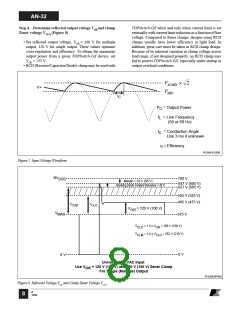
P = Output Power
O
f
t
= Line Frequency
(50 or 60 Hz)
L
= Conduction Angle
Use 3 ms if unknown
C
η = Efficiency
PI-2585-012500
Figure 7. Input Voltage Waveform.
BV
700 V
DSS
Margin = 53 V (95 V)
647 V (605 V)
627 V (585 V)
Blocking Diode Forward Recovery = 20 V
555 V (525 V)
495 V (475 V)
V
V
CLM
CLO
V
= 120 V (100 V)
OR
V
MAX
375 V
V
= 1.5 x V
= 1.4 x V
= 180 V (150 V)
CLO
CLM
OR
V
= 252 V (210 V)
CLO
0 V
0 V
Universal/230 VAC Input
Use V
= 120 V (100 V) and 180 V (150 V) Zener Clamp
For Single (Multiple) Output
OR
PI-3336-091402
Figure 8. Reflected Voltage VOR and Clamp Zener Voltage VCLO
.
B
12/02
8

 ETC [ ETC ]